


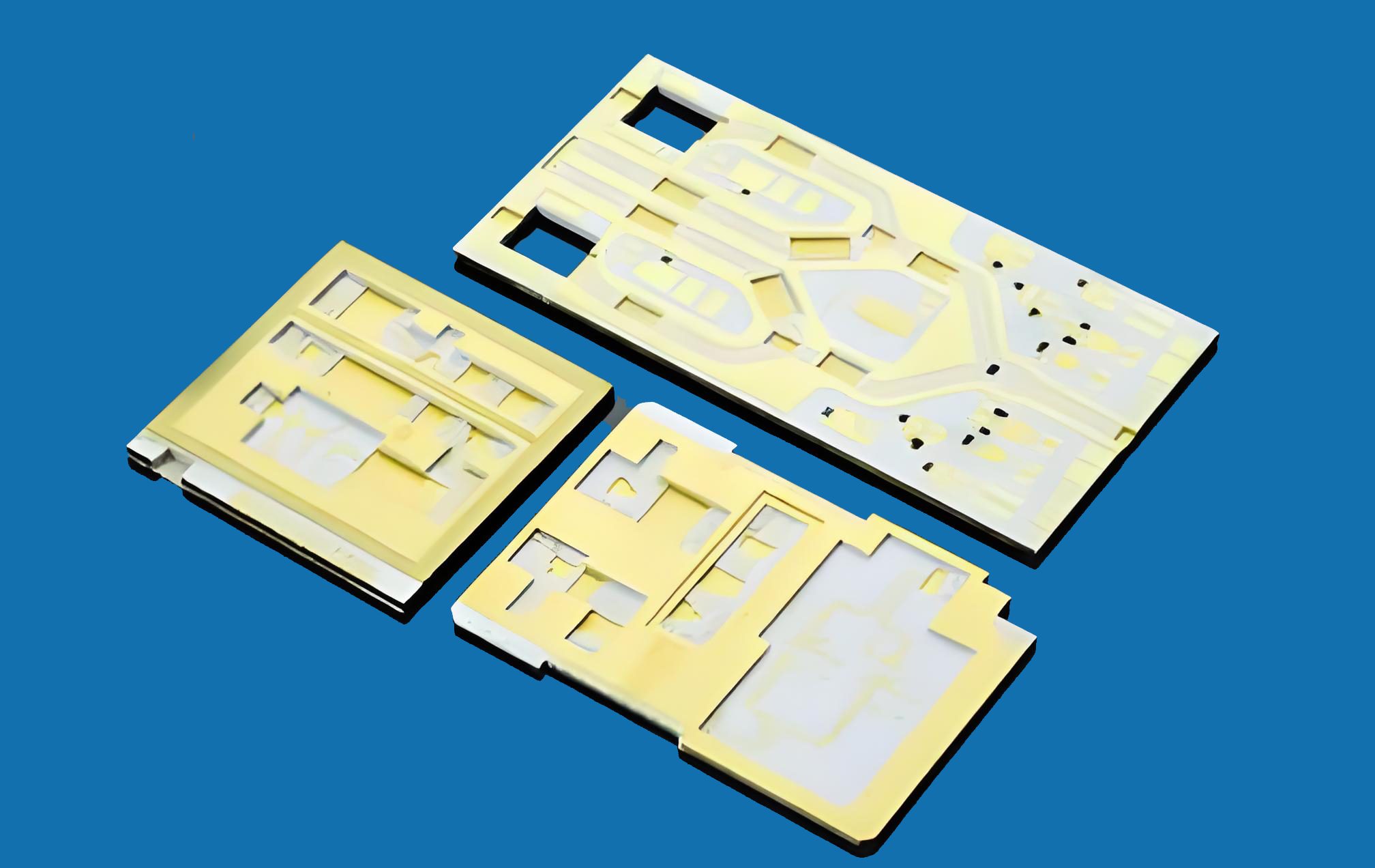
Ceramic substrates play a critical role in modern electronics, offering exceptional thermal performance, mechanical strength, and customization options. Alumina remains the most widely used material due to its affordability and versatility, while aluminum nitride is favored for applications requiring higher thermal conductivity. The choice of manufacturing process—whether HTCC, LTCC, DBC, DPC, or LAM—will depend on the specific needs of the application, including power electronics, electronic packaging, hybrid microelectronics, and multi-chip modules. With their outstanding thermal conductivity, mechanical stability, and electrical insulation properties, ceramic substrates play a pivotal role in developing advanced electronic devices.
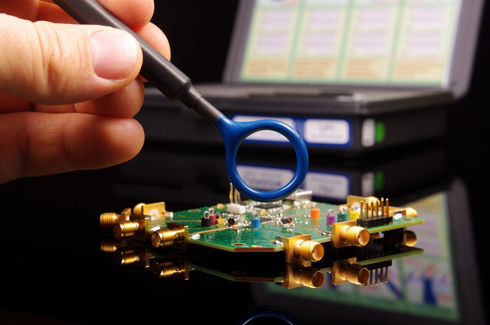
As electronic devices become more complex and ubiquitous, the need for reliable and high-performance PCBs continues to grow. PCB testing standards provide a framework for ensuring that these essential components meet industry benchmarks for safety, reliability, and functionality. Manufacturers who adhere to these testing standards are better positioned to deliver high-quality, dependable products, build trust with their customers, and minimize the risk of product failures. Whether through visual inspection, electrical testing, or advanced X-ray analysis, rigorous testing ensures that the PCBs will perform as expected, even in the most challenging environments.

As the largest PCB manufacturer globally, China not only leads in production volume and technology but also continues to innovate. By increasing research and development investment and optimizing production processes, China’s PCB industry has gradually transitioned from low-end manufacturing to high-end production, especially excelling in areas such as high-frequency, high-speed, and high-precision applications. Meanwhile, China’s cost advantages, rich industrial chain resources, and mature supply chain management systems further solidify its dominant position in the global market.
In conclusion, managing EMI and ensuring EMC are critical aspects of PCB design and manufacturing. By carefully considering factors like trace routing, grounding, component selection, and shielding, designers can minimize the risks associated with electromagnetic interference and create devices that perform reliably and safely.
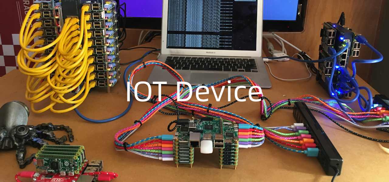
As IoT technology advances, so do the requirements for Printed Circuit Board (PCB) design and manufacturing. This blog extends the discussion on how IoT is driving innovations in PCB design, exploring deeper insights into new design techniques, material advancements, manufacturing challenges, and future prospects.
The Internet of Things (IoT) is revolutionizing industries worldwide, and its influence on Printed Circuit Board (PCB) design and manufacturing is profound. As IoT devices become more compact, efficient, and interconnected, the demand for innovative PCB designs has surged. This blog delves into how IoT is transforming PCB design and manufacturing, the challenges it poses, and the opportunities it presents.
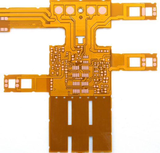
Flexible printed circuit boards (PCBs) are a cornerstone of modern electronics, found in devices like smartphones, cameras, and electric vehicles. Unlike traditional rigid PCBs made from FR4 (flame retardant material), flexible PCBs utilize polymer substrates such as polyimide, resulting in their signature amber or orange appearance
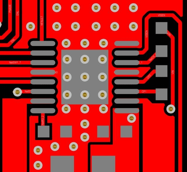
Motor driver ICs handle high currents and dissipate substantial heat, so efficient PCB design is essential to ensure proper heat dissipation and reliable performance. Below are some best practices for designing a robust PCB for motor driver ICs.
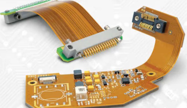
Flexible PCBs (printed circuit boards) provide the ability to bend and conform to various shapes, making them an essential technology for space-constrained and dynamic applications. A 2-layer flex PCB contains a flexible dielectric layer sandwiched between two conductive copper layers. Designing these PCBs requires unique considerations, including material selection, layout techniques, manufacturability, and reliability.
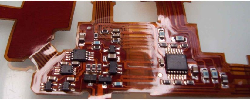
Flexible printed circuit boards (flexible PCBs or flex circuits) are made from flexible insulating materials such as polyimide film. Unlike traditional rigid PCBs, flexible PCBs can bend and twist while maintaining electrical connectivity, making them ideal for space-constrained and dynamic applications.