


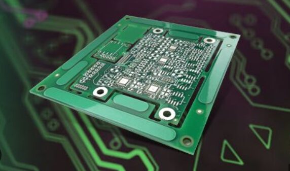
Proper PCB design requires careful planning and attention to detail, from schematic creation to component layout and wiring. Following these best practices ensures optimized signal integrity, reduces interference, and minimizes manufacturing issues, leading to higher-quality and more reliable PCB designs.
Understanding these common misunderstandings in circuit design is essential for engineers who want to improve efficiency, reduce power consumption, and design more reliable systems. By addressing these myths, you can avoid co
Electromagnetic compatibility (EMC) refers to the ability of electronic devices to function harmoniously in their electromagnetic environment without causing or being affected by electromagnetic interference (EMI). The goal of EMC design is to enable electronic devices to resist external interference while minimizing the electromagnetic interference they emit to surrounding devices
In circuit board manufacturing, various electroplating methods are employed to enhance performance, durability, and contact quality. This article focuses on four specialized electroplating methods commonly used in PCB (printed circuit board) welding processes
RF circuit board design is a critical and often complex area of PCB engineering. While there are many uncertainties in theory, practical design rules can be followed to optimize performance.
HDI boards represent the forefront of PCB technology, enabling smaller, more efficient electronic devices while meeting the demands of modern consumer electronics and telecommunications.
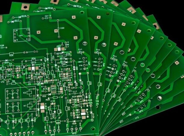
Printed Circuit Boards (PCBs) are the foundation of most electronic devices. The PCB production process can be categorized into subtractive methods and additive methods. Currently, the most commonly used industrial method is the copper foil etching process, a subtractive method.
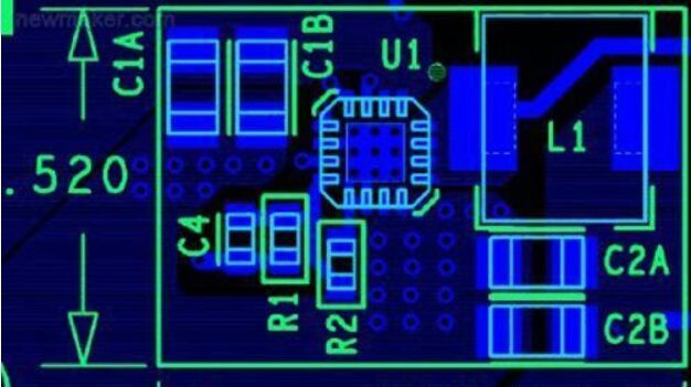
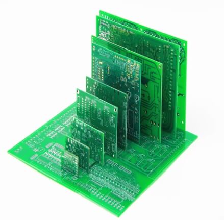
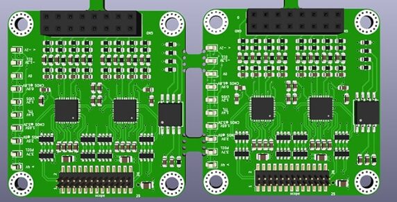
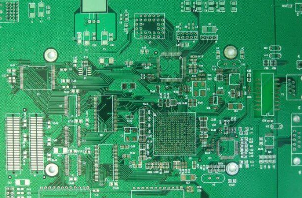
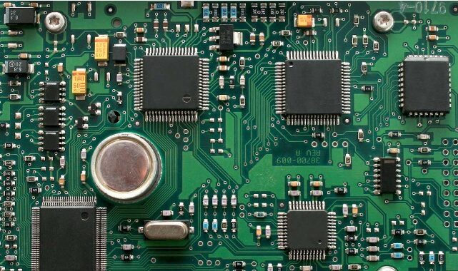
PCB design involves two critical stages: component layout and circuit connection wiring. The layout is the arrangement of circuit components within the PCB’s wiring area. A well-thought-out layout directly affects the ease of subsequent wiring and significantly impacts the PCB’s overall performance. In addition to meeting circuit functionality and performance requirements, a good layout considers manufacturability, inspection, and maintenance. Components should be placed evenly, neatly, and compactly, ensuring that leads and connections are short, minimizing interference and signal transmission delays.
At KKPCB, we offer reliable electronic components sourcing, streamlining the process for you. Send us your BOM, and we’ll handle everything, eliminating the need for you to compare prices and sources.
- 1
- 2