


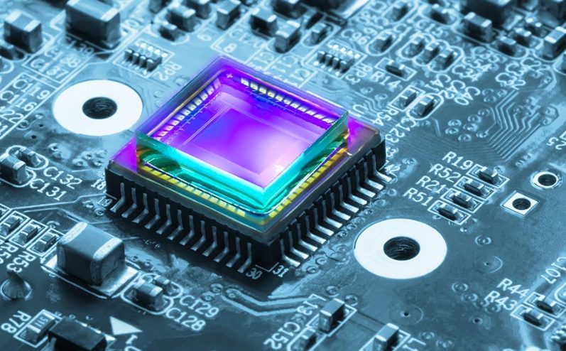
Sensors and transducers play integral roles in PCBs by enabling electronic systems to interact with and respond to the surrounding environment. Sensors detect physical parameters such as temperature, pressure, light, and motion, converting these analog signals into electrical signals that PCBs process. Sensors are used in various applications, from environmental monitoring and industrial automation to consumer electronics.
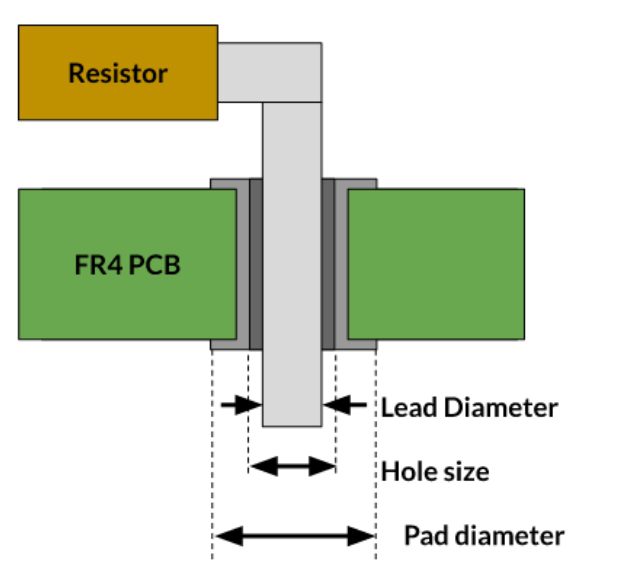
In printed circuit board (PCB) design, the choice of pad type plays a critical role in determining the durability, reliability, and performance of the final product. Through-hole pads, which are designed for components with leads that pass through the PCB, offer superior mechanical and electrical connections compared to surface mount pads.
Printed Circuit Board (PCB) routing is a critical aspect of electronic design, ensuring that electrical signals are transmitted efficiently and reliably between components. Proper routing minimizes interference, maintains signal integrity, and meets design requirements such as impedance control and thermal management. This article outlines the best practices for PCB routing, focusing on optimizing performance and ensuring signal integrity.
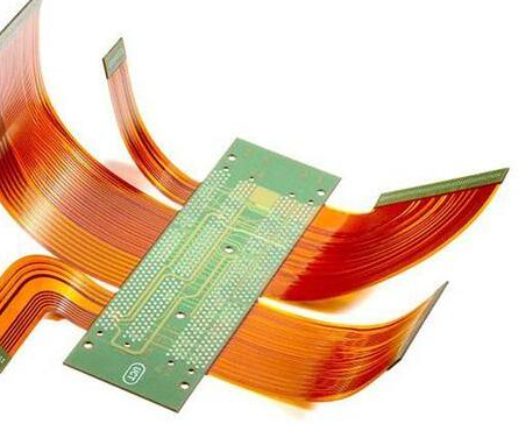
Rigid-flex PCBs represent a groundbreaking advancement in electronics design, combining the best features of rigid boards and flexible circuits. By integrating high-density interconnect (HDI) technology, rigid-flex PCBs eliminate the need for traditional board-to-board connectors and simplify assembly processes.
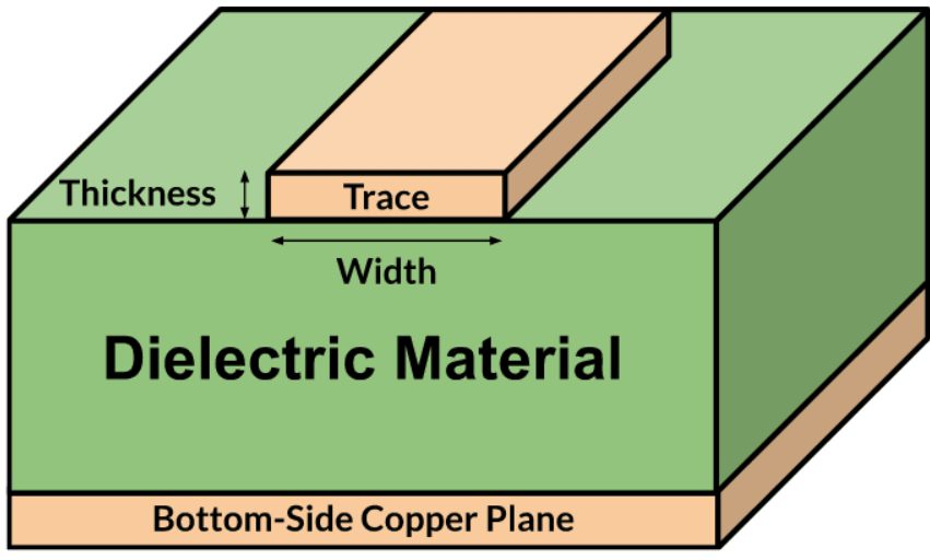
The relationship between PCB trace thickness and current capacity is a critical aspect of PCB design. Properly sizing traces ensures that they can handle the required current without overheating, which is essential for the reliability and functionality of the circuit. This article explores the key considerations for selecting trace thickness, the impact of copper weight, and methods for calculating current capacity, along with design strategies for high-current applications
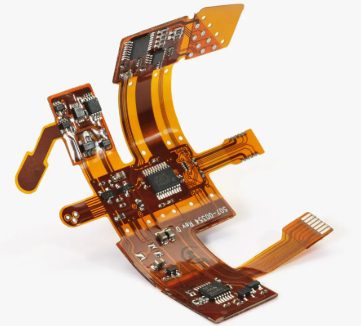
As the demand for flexible and rigid-flex PCBs continues to grow, understanding the factors that influence their cost is crucial for optimizing designs and ensuring cost-effective production. Rigid-flex PCBs offer significant advantages, such as enhanced flexibility, reliability, and space-saving capabilities, but they also come with unique challenges that can drive up costs if not properly managed. This article explores key design considerations, cost factors, and strategies for optimizing rigid-flex PCB designs.
High-density interconnect (HDI) PCBs have become a standard in modern electronics, enabling designers to create smaller, more functional devices. However, designing HDI PCBs requires careful attention to detail due to their complexity and the advanced technologies involved. This article outlines key HDI PCB design guidelines, highlights the advantages and disadvantages of HDI layouts, and provides insights into overcoming common challenges.
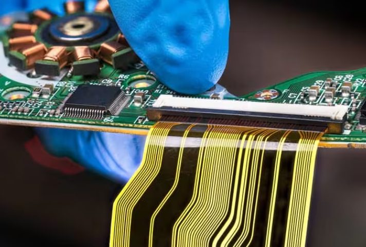
Flexible PCBs, commonly made from polyimide materials, are known for their amber color and ability to withstand high temperatures, often comparable to or exceeding those of FR4 boards. The current carrying capacity of flexible PCBs is primarily determined by factors such as copper thickness, trace width, and material properties.
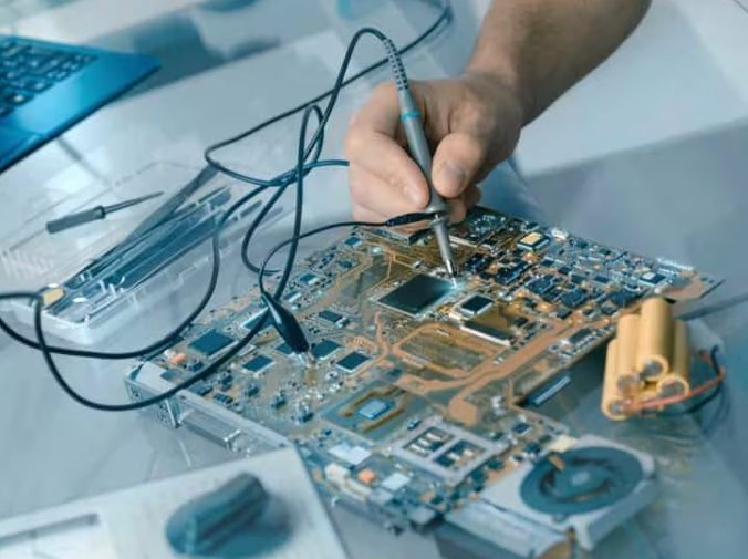
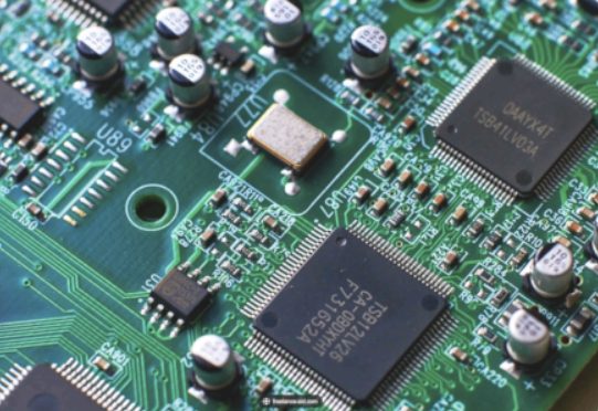
Troubleshooting printed circuit boards (PCBs) can be a daunting task, but with a systematic approach, it becomes manageable and efficient. This guide provides a step-by-step process to identify faulty components on PCBs, along with methods tailored to specific component types and advanced techniques for batch inspection.
Creating a robust component library is one of the most challenging yet critical aspects of PCB design. The quality of the library, which includes schematic symbols, PCB footprints, and 3D models, directly impacts the success of your board development. Among these, the PCB footprint plays a pivotal role in determining whether your board can be manufactured and assembled correctly.