


Practical Tips for Non-Direct Replacement
Double-check pin numbering to avoid miswiring.
Adjust external PCB components to suit the replacement IC’s characteristics.
Match power supply voltage; if it differs, adjust accordingly.
Measure IC’s static working current post-replacement for normal values; significant differences may indicate self-oscillation.
Match input and output impedance to the original PCB circuit.
Maintain tidy external leads and avoid crossings to prevent high-frequency oscillation.
In the ever-evolving landscape of electronics, high-frequency printed circuit boards (PCBs) are crucial for enabling advanced communication technologies. Among the materials dominating this sector, Rogers 6010 and aluminum-based substrates stand out for their unique properties and performance capabilities. This article explores the characteristics, advantages, and applications of these materials, shedding light on their significance in modern electronics.
In PCB design, one common question arises: if an extra layer is not required for routing, why use it? Reducing the number of layers theoretically makes the board thinner and lowers costs. However, in some cases, adding an additional layer can actually reduce costs.
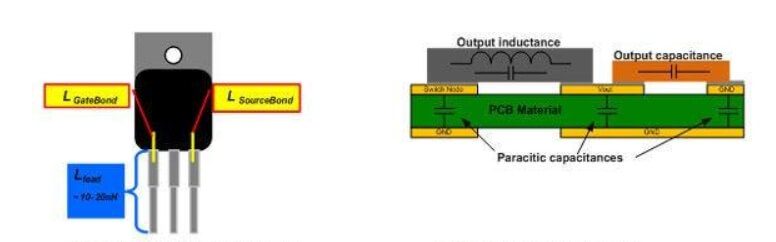
Based on recent trends, improving efficiency is a key goal, and the trade-off of using slow switching devices for better EMI is not worth it. Superjunctions can improve efficiency in applications where planar MOSFETs struggle. Superjunction MOSFETs significantly reduce on-resistance and parasitic capacitance compared to traditional planar MOSFET technology. The significant reduction in on-resistance and reduced parasitic capacitance, while helping to improve efficiency, also produces fast switching transitions of voltage (dv/dt) and current (di/dt), forming high-frequency noise and radiated EMI.
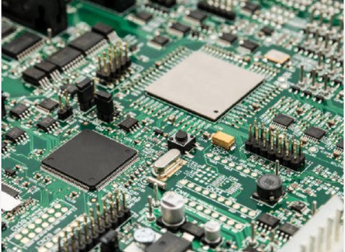
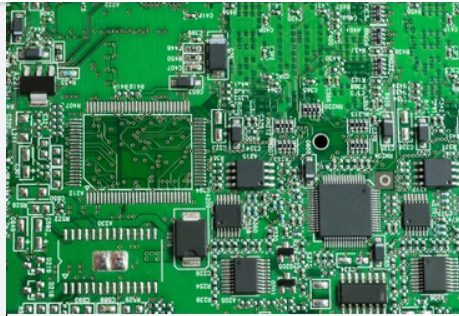
In today’s technology-driven world, the Printed Circuit Board (PCB) stands as a foundational component in electronic devices. From smartphones to complex medical equipment, PCBs are essential for ensuring reliable electrical connections and functionality. This article delves into the critical stages of PCB design, manufacturing, and final artwork, providing insights into the complexities and technicalities of creating effective circuit boards.
As electronic products become more advanced, they encounter more sources of electromagnetic interference (EMI) that can disrupt device function and potentially harm health. This guide explores strategies for designing PCB boards with optimized electromagnetic compatibility (EMC), focusing on reducing interference and increasing product resilience.
Electrostatic Discharge (ESD) can damage sensitive components such as MOSFETs, CMOS gates, and PN junctions, leading to issues like gate damage, short circuits, and even melted wiring. This guide offers practical strategies to design PCBs that effectively prevent ESD from harming the circuit.
Before explaining the inspection work after PCB wiring is completed, we will first introduce three special PCB routing techniques. The routing of PCB LAYOUT will be explained from three aspects: right-angle routing, differential routing, and serpentine routing
PCB design translates electrical schematics into a functional product, and its quality directly impacts production efficiency and product reliability. For beginners, mastering PCB layout can be challenging despite familiarity with design software, and common issues often arise. Here, seasoned engineers from KKPCB share their PCB layout insights to help avoid these pitfalls and inspire best practices.
Addressing signal integrity (SI) issues early in the PCB design process can streamline the design and eliminate the need for corrective termination devices later. Here, we outline critical steps to maintain signal integrity, from planning through testing.