


Client Industry: European EMC Testing Equipment Manufacturer Applications: ISO 17025-Certified Probe Calibration / High-Frequency Field Measurement 1. Manufacturing Challenges Critical Requirements: Previous Supplier Limitations:▶ Manual thickness compensation caused ±8% dielectric variation▶ PTFE delamination during lamination (yield loss 15%)▶ Probe-to-probe measurement deviation >±3.5dB 2. Precision Manufacturing Innovations (A) Proprietary Process Flow Process Stage Technical Breakthrough Control Precision Material Prepreg […]
Client Industry: European Industrial Equipment ManufacturerApplications: Particle Accelerator RF Systems / Industrial Microwave Heating 1. Industry Manufacturing ChallengesCritical Requirements: Previous Supplier Issues:▶ CTE mismatch in traditional aluminum substrates caused copper layer delamination▶ Manual MOSFET soldering led to ±15% thermal resistance variation▶ Water-cooling solutions increased system complexity by 30% 2. Advanced Manufacturing Solutions (A) Core Process […]
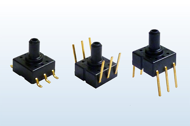
1.Background Overview
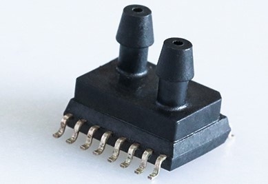
A client from Europe, engaged in the development of industrial automation systems, required integration of a high-precision pressure sensor module in their next-generation process control system. The module needed to detect subtle changes in gas or liquid pressure in real time to enable dynamic control and safety alerts.
Given the complex environment in which the equipment would operate, the client emphasized strict standards for PCB heat resistance, soldering reliability, and circuit stability.
KKPCB was selected as the PCBA manufacturing partner for this project due to our rich experience in industrial control applications and our proven ability to deliver high-reliability solutions.
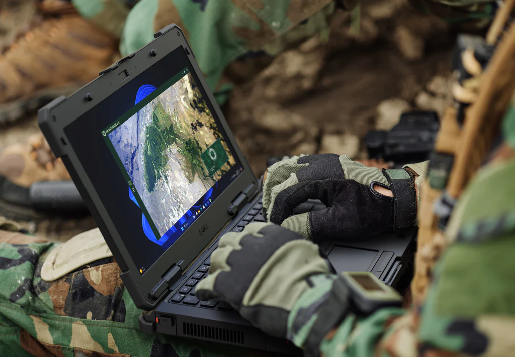
Industry: Defense Electronics
End Applications:
Armored vehicle main control units
Field communication relay equipment
Manufacturing Challenges:
Heterogeneous material processing (AlSiC metal substrate + FR4 multilayer hybrid lamination)
Extreme environment reliability (MIL-STD-810H vibration compliance)
Military-grade quality control (100% inspection + batch traceability)
Previous Supplier Pain Points:
✔ AlSiC substrate yield only 65% (delamination due to CTE mismatch)
✔ PCIe gold finger contact failure rate 3,000 PPM (post-vibration)
✔ EMP shielding layer vacuum lamination yield below 80%
1. Project Background
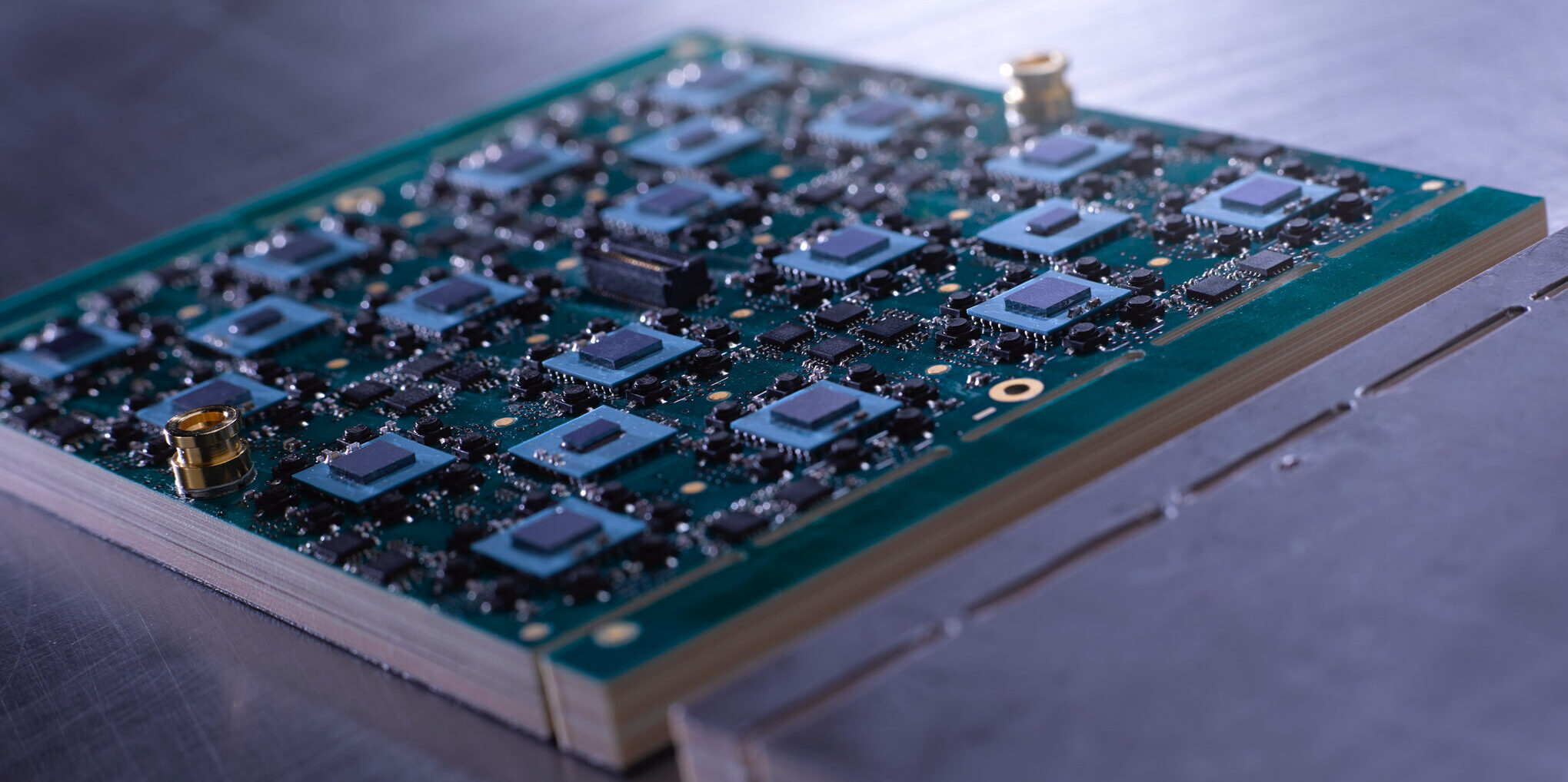
Industry: Satellite Communications/Military Radar
Application Scenario:
256-channel phased array antenna system (28GHz Ka-band)
Customer requirements: ±60° beam steering, ±0.5dB amplitude consistency, 8-week delivery
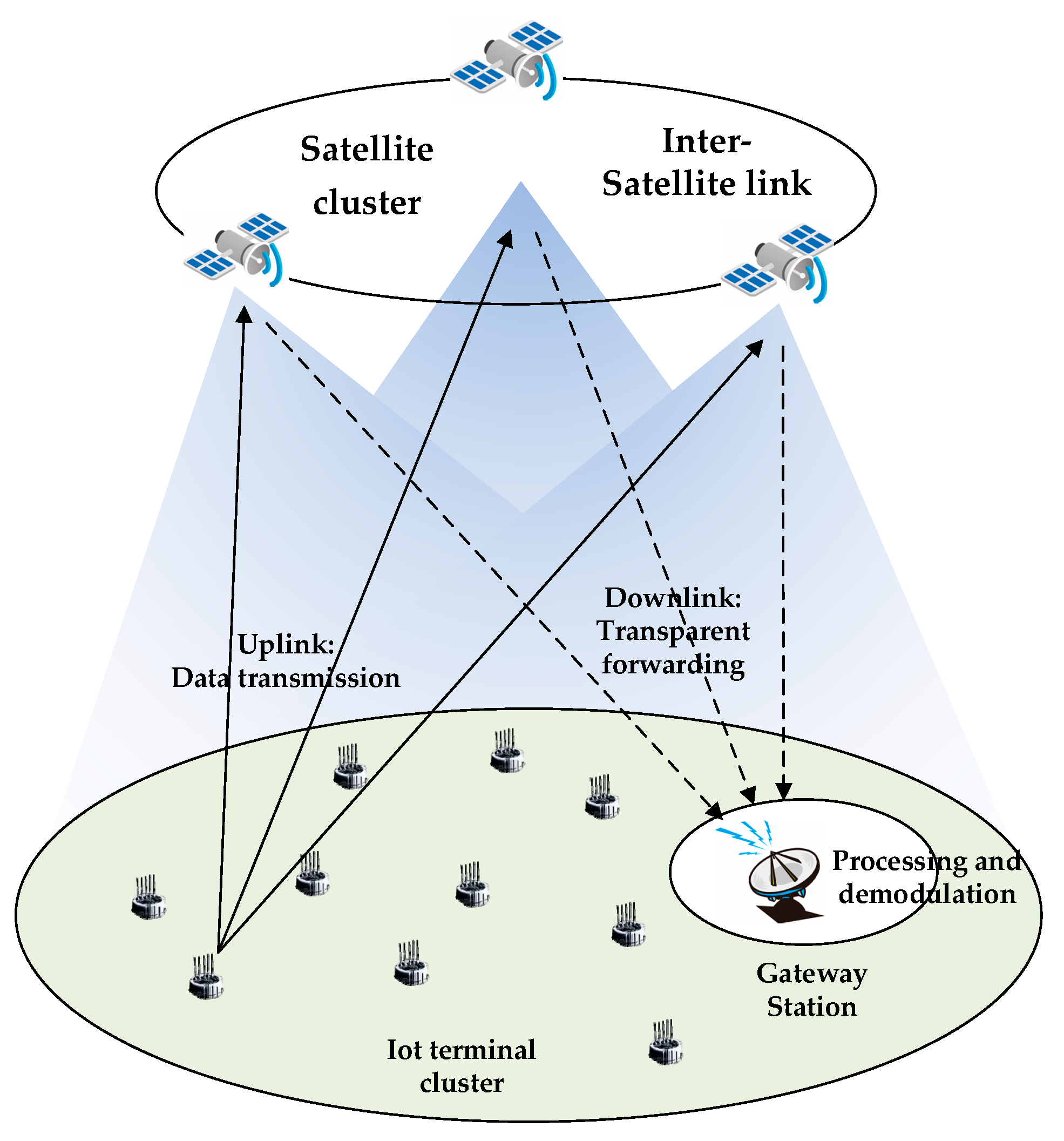
(ASTM E1647 Validated, 60% Cost Reduction vs. Ceramic Substrates) Project Introduction This project developed a mission-critical PCB for commercial satellite IoT terminals requiring: “The Rogers/Taconic hybrid stackup solved our insertion loss and CTE mismatch problems simultaneously.”— Lead RF Engineer (Client R&D Team) Key Specifications Parameter Target Achieved Frequency Range 902-928MHz (LoRa) + 1.5GHz (SatIoT) 850MHz-1.6GHz […]

1. Customer Profile Client: AnonymousIndustry: ADAS (Advanced Driver Assistance Systems), Autonomous VehiclesApplication: 77GHz Long-Range Radar (LRR) for Highway Pilot & Collision Avoidance Customer’s Requirements: Key Challenges: 2. KKPCB’s Radar PCBA Solution (A) Material & Stackup Layer Material Function Key Specs RF Layers Rogers RO3003 Antenna Array & Front-End Dk=3.0, Df=0.0013 @ 77GHz Core Arlon 25FR […]
1️⃣ Background Overview Global medical equipment is accelerating its intelligentization, and the requirements for the accuracy and reliability of pressure sensors in ventilators continue to increase. A Middle Eastern medical equipment manufacturer plans to upgrade its ventilator airway control system, which requires a differential pressure sensor module that can operate stably in a high temperature and […]
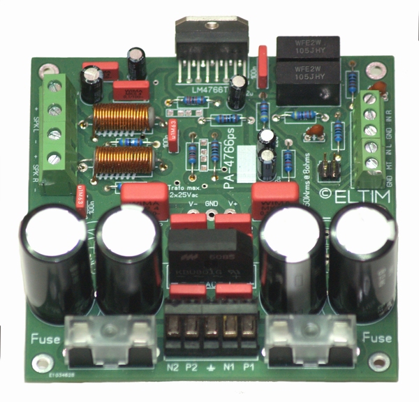
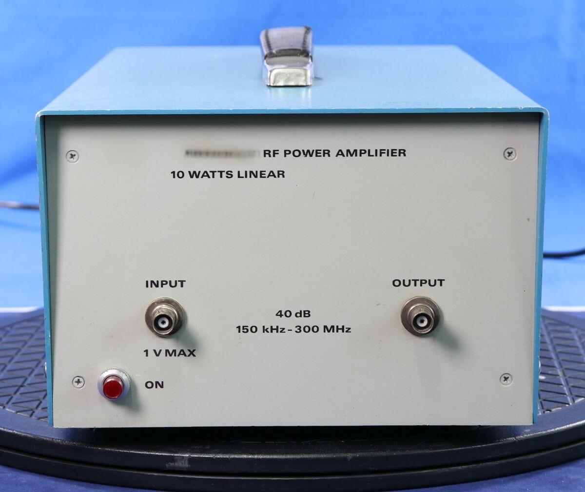
Client: A leading European audio equipment manufacturer
Industry: High-End Consumer Audio / Professional Sound Systems
Application: Stereo Power Amplifier Modules
Client: Anonymous
Industry: Telecom Infrastructure, 5G Macro/Micro Base Stations
Application: Power Amplifier (PA) Modules + RF Front-End PCBs
High-power base station equipment requiring PCBs are able to handle:
High current (30A+) for PAs
Low-loss RF (3.5GHz-28GHz for 5G)
Thermal stability (85°C ambient, 125°C local hotspots)
Key Challenges Faced:
Delamination risk from mixed thick-copper (6oz) and RF layers.
EMI coupling between power and RF sections.
Thermal warping under high thermal cycling.