


Client: Anonymous
Industry: Fiber Optic Test & Measurement, High-Speed Data Transmission
Application: Next-gen 100G/400G+ optical transceivers, OTDR equipment, and 50GHz RF test modules.
FIS designs precision fiber optic tools, requiring ultra-low-loss PCBs to maintain signal integrity at millimeter-wave frequencies (up to 50GHz). Their challenges include:
Insertion loss degrading high-speed signals (>40Gbps).
Impedance mismatches causing reflection noise.
Thermal expansion leading to microvia cracking in compact designs.
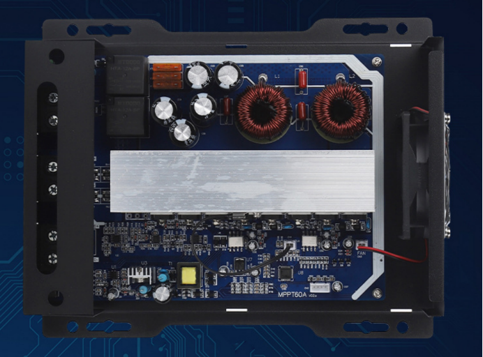
Project Background A manufacturing plant in California sought to reduce electricity costs through a distributed rooftop solar system while enhancing its green and sustainable corporate image. With ample rooftop space available, the company required a highly efficient MPPT solar controller capable of maximizing solar energy utilization and ensuring stable operation. ⚡The Role of PCBA Technology […]
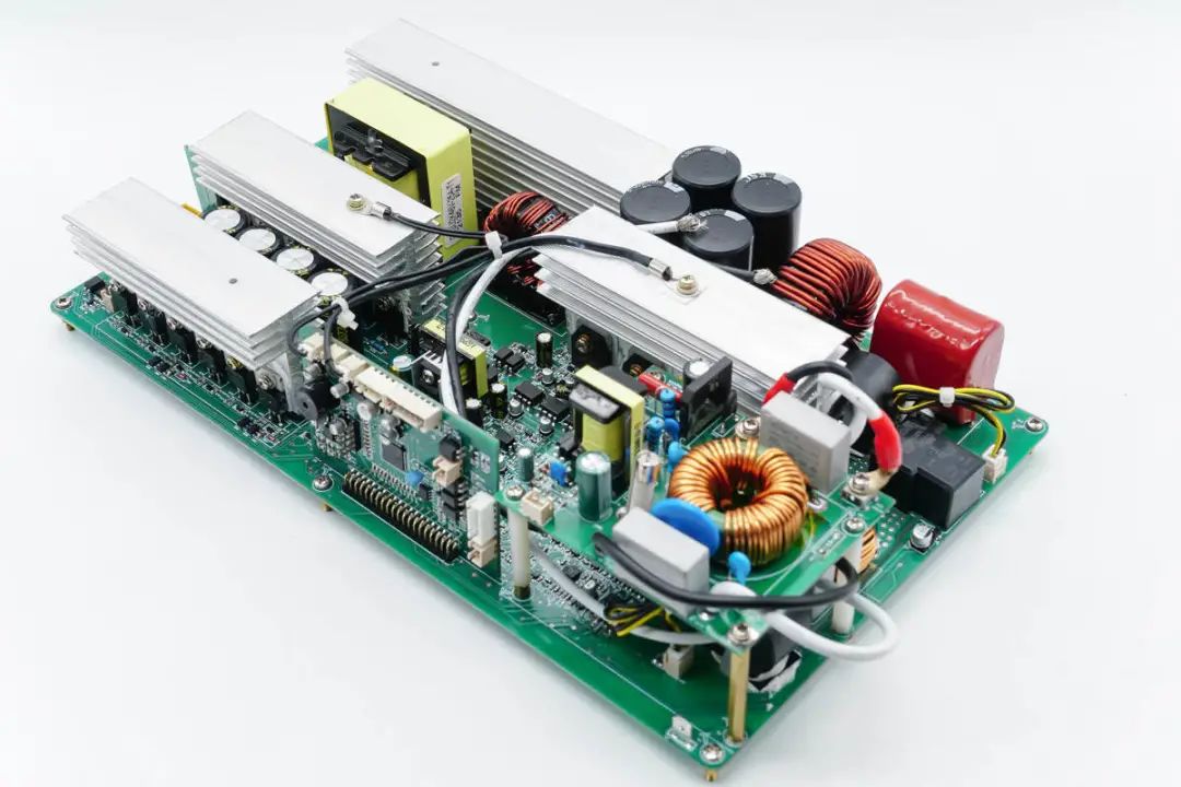
Optimizing Small Wind Turbine Inverters: Enhancing Stability & Reliability Customer Background & Market Demand Germany is a global leader in renewable energy, with its Energiewende (energy transition) policy driving widespread adoption of distributed wind power for rural electrification, industrial parks, and off-grid energy solutions. Small Wind Turbines (SWTs) have become an essential power supply option […]

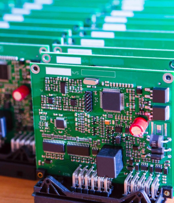
The customer is a globally leading manufacturer of communication equipment, specializing in the development and production of large-scale routers, switches, servers, and high-speed networking devices. As modern network communications demand increasingly high signal integrity, reliability, and thermal stability, the customer required an 18-layer PCB with low-loss material (S1000-2M) and advanced immersion gold plating to ensure stable signal transmission and long-term reliability
When designing a PCB, one of the critical decisions you’ll face is whether to use plated or unplated mounting holes. These holes are essential for securing the PCB to an enclosure or package, but the choice between plated and unplated holes depends on your design requirements, grounding needs, and mechanical considerations. Let’s explore the differences, advantages, and best practices for each type.
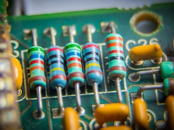
PCB resistors are designed to be mounted and soldered to printed circuit boards; they control current flow and divide voltages, among other things. PCB resistors come in many shapes and sizes, but they’re all designed to fit easily into board layouts. They have two terminals that can be soldered to the conductive traces on the PCB so they can be connected electrically to the rest of the circuit.
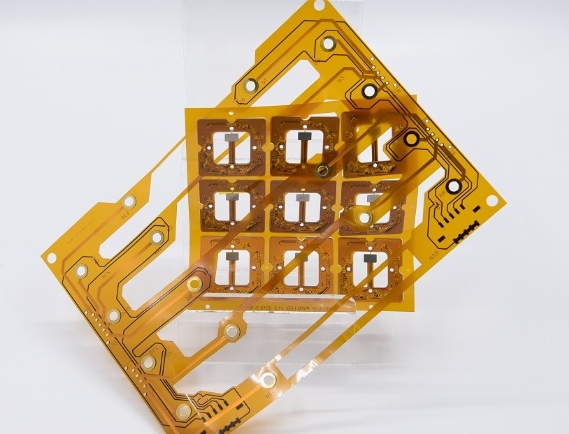
It wasn’t long ago that rigid circuit boards were the only possible electronic system method available. Whether it was entertainment or industrious, the shape of most devices was an extension of an intractable rigid board. More recently, the tide has turned: as technology has developed and matured, the enclosure is shaping the electronics inside them. Despite additional manufacturing challenges, flexible PCBs (or flex printed circuits) are enticing to product designers due to a nearly unlimited range of possibilities compared to rigid board constraints.
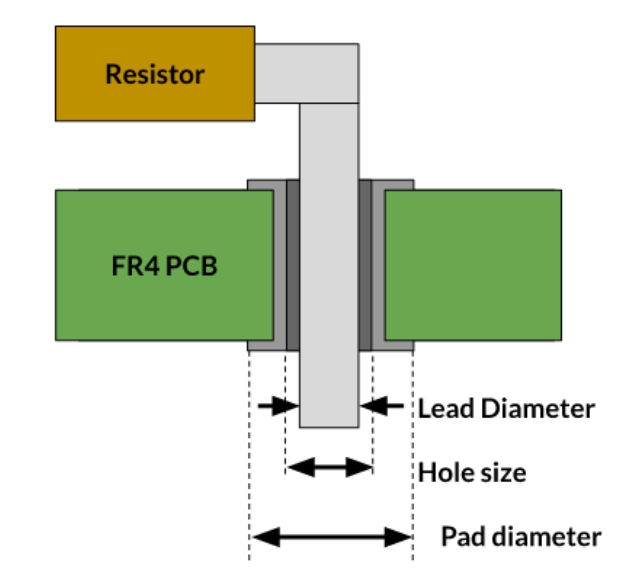
In printed circuit board (PCB) design, copper pads are points for attaching components with soldering. These pads come in two primary types: through-hole and surface-mount (SMD). Through-hole pads are designed for components with leads that are inserted through the pad’s holes and soldered on the opposite side of the board. This method ensures a mechanical and electrical bond between the component and the PCB, beneficial for long-term reliability. Read on as we discuss through-hole pad design.
PCB routing involves laying out traces to minimize interference, ensure signal integrity, and meet design requirements such as impedance control and thermal management. Traces carry electrical signals between components such as integrated circuits, resistors, and capacitors. PCB traces are usually made of copper.
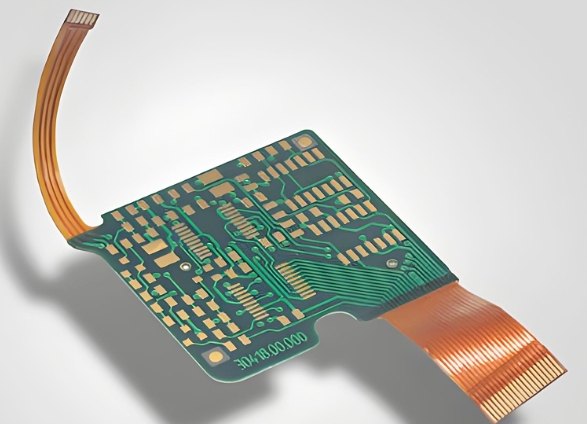
Combining the flexibility of flex circuits with the robustness of rigid boards, while leveraging High-Density Interconnect (HDI) technology, represents a significant breakthrough in modern electronics. Traditional methods like board-to-board stacking connectors or standard flex circuits often present challenges, such as cumbersome assembly and potential damage during connection. Rigid-flex PCBs offer a seamless solution, eliminating these bottlenecks and enabling more efficient designs.