


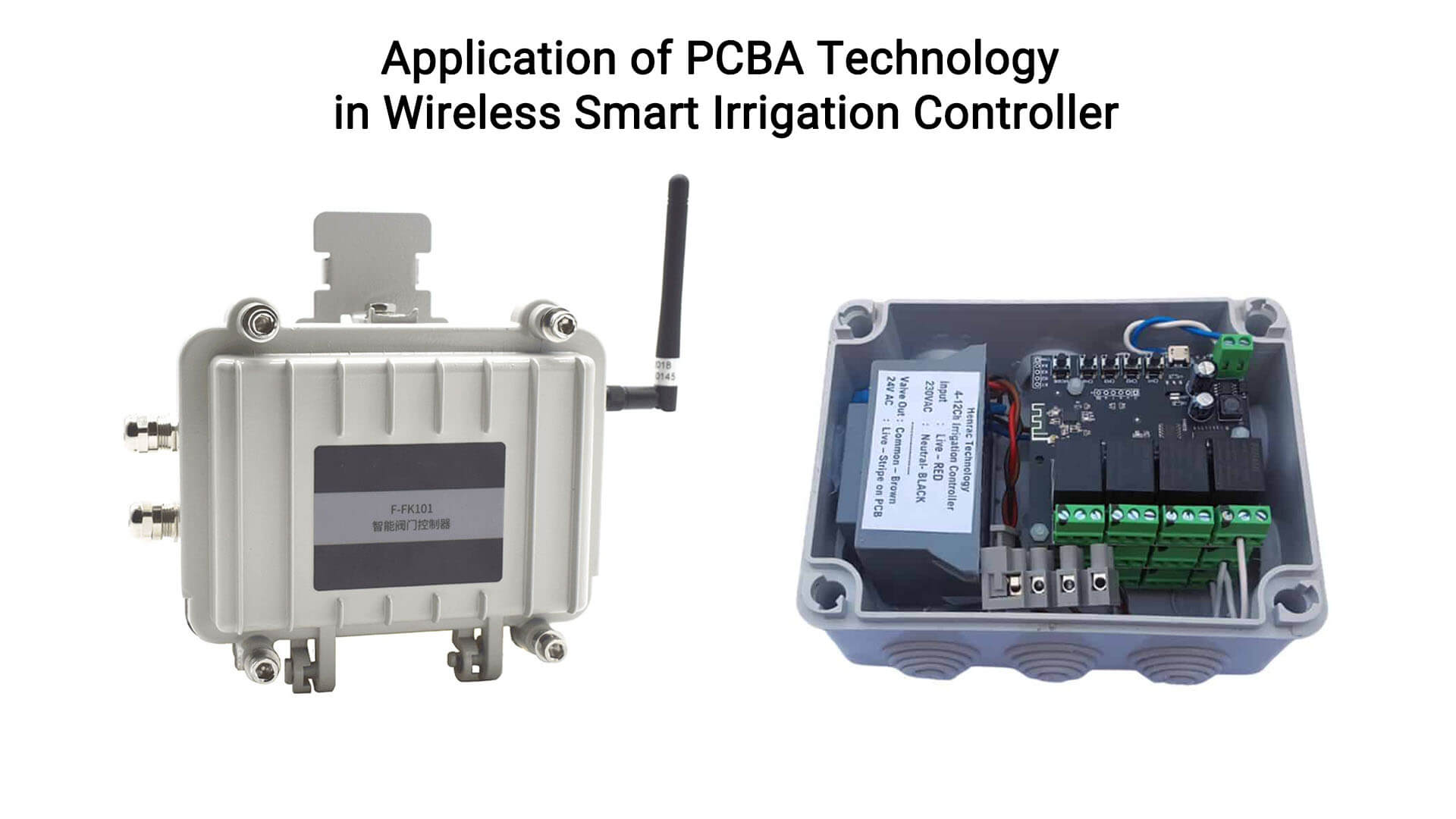
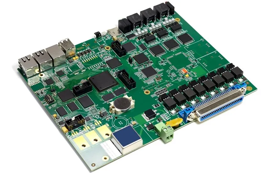
With the increasing global water scarcity, especially in large-scale agricultural planting areas, traditional irrigation methods face issues such as water waste, cumbersome manual operations, and imprecise irrigation control. To address these pain points, we have helped our customers develop a wireless smart irrigation controller PCBA.
These PCB tolerances ensure that PCB circuit boards are produced precisely and can function as intended. Manufacturers adhere to specific in-house tolerance guidelines, based on international standards like IPC-A-600 Class 2, to maintain quality throughout the production process.
Electronics are becoming faster, smaller, and used in more demanding environments. Miniaturized ICs and SMDs operate at higher frequencies and require more power. Increased current demands cause voltage drops across resistive elements, generating heat and leading to temperature rises and hotspots. Over half of electronic component failures now stem from heat-related stress.
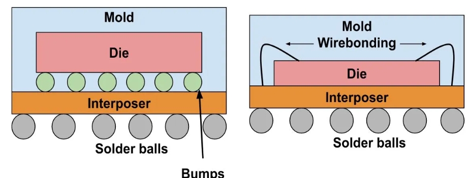
Chip-Scale Package (CSP) is a type of integrated circuit packaging technology. The size of the package is up to 1.2 times the size of the actual die, with only a single-die and a direct surface mountable package. First originating in the 1990s, it was developed as a response to the demand for smaller and more efficient packages.
Take a look at any type of multiconductor serial bus that uses single ended traces. You’ll probably see some resistors sitting around the bus being connected to driver pins and power or ground. The use of these resistors is intentional with the purpose being to set the signal level and reflection control on the bus. The other reason is placement as a pull-up resistor, where a line in the bus is pulled up to the signal power supply level.
When designing for PCB prototyping, the cost of individual parts does not always play a big role. If you’re designing one-offs or hobby projects, you’ll probably only look at parts prices when your assembly house sends you an invoice.
PCB edge plating is a specialized process that involves applying a metal coating to the exposed copper connections at the edge of a printed circuit board (PCB). This technique, also known as side plating, battlement, or metallized edge plating, enhances electrical connectivity, structural rigidity, and electromagnetic interference (EMI) shielding.
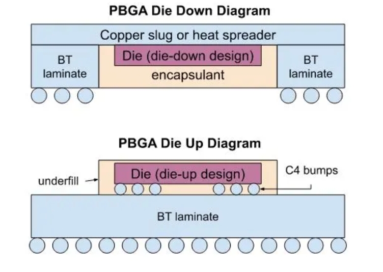
A ball grid array (BGA) is a type of surface-mount packaging that features an array of small solder balls on the underside, which serve as electrical connections to the printed circuit board (PCB). Unlike dual in-line or flat packages, ball grid arrays offer the advantage of accommodating a greater number of interconnection pins, made possible by utilizing the entire bottom surface of the device for connections instead of only relying on the perimeter
Manual soldering, while not as precise as automated assembly processes like reflow soldering, is still widely used in various applications. However, it is prone to specific defects that can affect the quality and reliability of the final product. Understanding these common manual PCB soldering defects is crucial for maintaining high product quality and yield
The Rogers RO4835 + IT180 hybrid PCB offers unparalleled performance for high-frequency and microwave applications, combining the best attributes of both materials. From automotive radar systems to advanced wireless communication and military-grade electronics, this hybrid PCB is optimized to meet the performance, durability, and reliability requirements of modern technologies.