


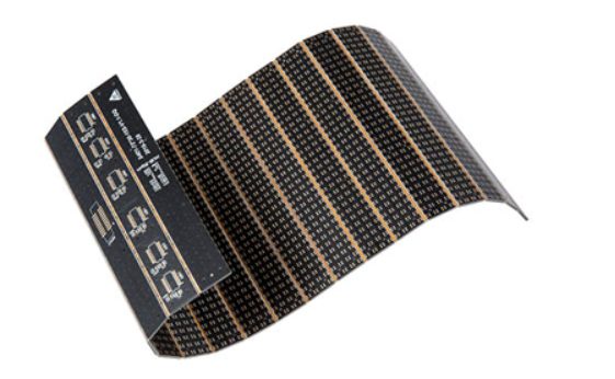
Rigid-flex PCB boards are one of the most widely used printed circuit boards for industrial applications. Their versatility is one of the main reasons for their popularity. They are made of a mix of rigid board and flex circuits, which means that the manufacturing method is similar to that of rigid board, but the circuit has a flexible circuit layer running through it.
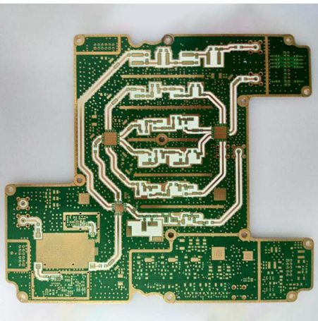
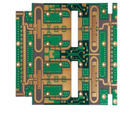
RF printed circuit boards are a highly complex but rapidly growing segment of the PCB manufacturing industry. In the PCB industry, boards that operate at frequencies above 100MHz are classified as RF PCBs. However, this standard stops at 2GHz. In addition, any board that operates at frequencies above 2GHz is called a microwave board.
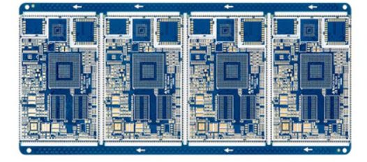
A printed circuit board, commonly known as a PCB, is an assembly that uses copper conductors and electricity to create electrical connections between electrical components. PCB manufacturers use a substrate to make it, which houses the components that form the basis of the PCB. PCBs are made of a variety of substrate materials, depending on the requirements of the circuit.
Radar PCBs are described as PCB substrates designed for radars. These PCBs are essential for communication circuits and detection. Radar PCBs use high-frequency PCB materials. Since they are used for communication and detection circuits, radar PCBs need to be highly efficient and operate at higher frequency outputs than standard PCBs. They are designed to send and receive radio frequency signals.

Solar energy is rapidly gaining popularity as an alternative energy source. One of the key components of a solar energy system is the solar inverter. A solar inverter is a device that converts the direct current generated by solar panels into alternating current

In the rapidly evolving healthcare industry, technology is the backbone of innovation and improved patient outcomes. Among these technological advancements, medical printed circuit board (PCB) assembly is a vital element driving progress in modern medical devices. With unmatched precision, reliability, and connectivity, medical PCB assemblies have become essential in reshaping healthcare delivery.
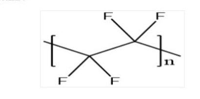
PCB boards are made of a variety of materials that can be used for high-frequency and high-speed applications: hydrocarbon resins, PTFE, LCP (liquid crystal polymer), PPE/PPO etc.
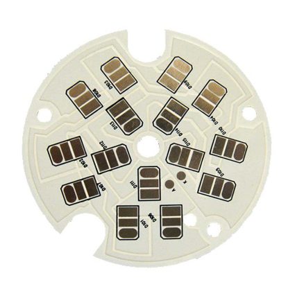
When selecting the right substrate for your printed circuit board (PCB), understanding the key differences between aluminum PCBs and FR4 PCBs is crucial.
Printed Circuit Boards may be used in various ways in the automobile industry, and the sky is the limit. The use of Automotive PCBs connections to power autonomous, self-driving cars has generated a lot of interest in the industry because of the potential savings in transportation costs and the increased speed and safety of product delivery.
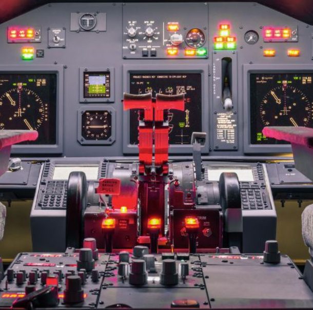
Both the military and aerospace industries require highly advanced electronics. Aerospace and military electronics require excellent reliability, quality, and compliance standards.