


As electronic devices become increasingly miniaturized, advancements in component and wiring technologies have created new challenges for production testing. Highly integrated ICs, smaller insulation spacings, and limited access to circuit nodes have made traditional testing methods insufficient. To address these challenges, a design-for-testability (DFT) approach is essential to reduce testing costs and enhance production efficiency. This guide explores the principles, strategies, and best practices for improving PCB testability.
Understanding the classification and parameters of PCB materials is essential for selecting the right material for a specific application. Factors like flame retardancy, Tg, resin type, and base material play critical roles in the performance and reliability of PCBs.
The quality of SMT laser steel mesh depends on factors like manufacturing process, material selection, design precision, and maintenance. By adhering to best practices in cleaning, storage, and handling, you can ensure optimal stencil performance and longevity.
Grounding is a critical aspect of PCB design, particularly in mixed-signal environments where digital and analog circuits coexist. Proper grounding ensures stable performance, minimizes noise, and improves the reliability of the overall circuit. Below are key insights and guidelines to address grounding challenges effectively.
In power supply design, PCB layout plays a critical role in ensuring the circuit’s efficiency, stability, and reliability. Below are five essential considerations for effective PCB design in power supply applications:
Proper packaging plays a crucial role in ensuring the safe delivery of PCBs, particularly in competitive markets where quality and presentation are key factors. Though packaging may not generate direct added value, it impacts customer satisfaction and reflects professionalism, particularly for high-precision products like PCBs.
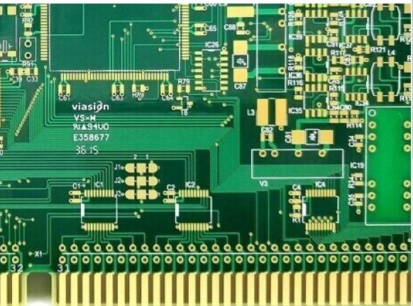
The interconnection of electrical contacts between components and electromechanical parts in a PCB ensures the system functions as per the circuit schematic. Selecting an appropriate interconnection method depends on the specific application, balancing reliability, processability, and cost. Below are commonly used PCB interconnection methods, along with their advantages, considerations, and application scenarios
Train personnel to consistently cut boards following the structural texture direction. If size variation persists, consider alternative substrate materials.
Work with laminate manufacturers to determine proper stress-relief processes before production.
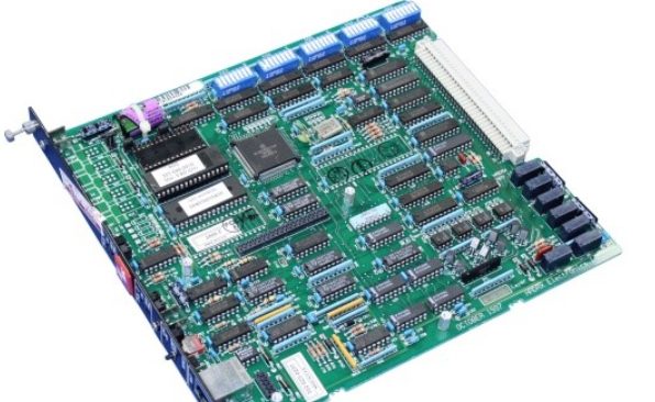
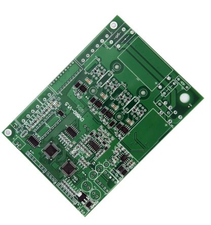
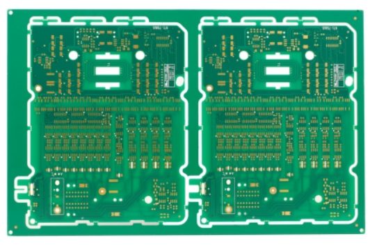
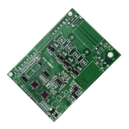
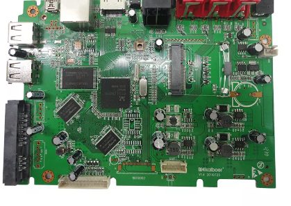
Often, products come without a circuit schematic, making it challenging to understand the PCB’s functionality and design principles. When faced with such a situation, follow these steps to reverse-engineer and restore the circuit diagram. This guide provides detailed instructions for accurately translating a physical PCB back into a schematic diagram.
PCB manufacturing relies on standardized guidelines to ensure consistent quality and reliability across various applications. The following list covers the most widely recognized standards from the IPC, EIA, and JEDEC organizations, essential for quality assurance in PCB design, assembly, and testing.