


Mastering these PCB design rules—like efficient grounding, proper trace sizing, and capacitor placement—significantly improves design quality and efficiency. By following these guidelines, you can reduce rework, save costs, and achieve more reliable, higher-quality PCB designs
Electromagnetic compatibility (EMC) refers to the ability of electronic devices to function harmoniously in their electromagnetic environment without causing or being affected by electromagnetic interference (EMI). The goal of EMC design is to enable electronic devices to resist external interference while minimizing the electromagnetic interference they emit to surrounding devices
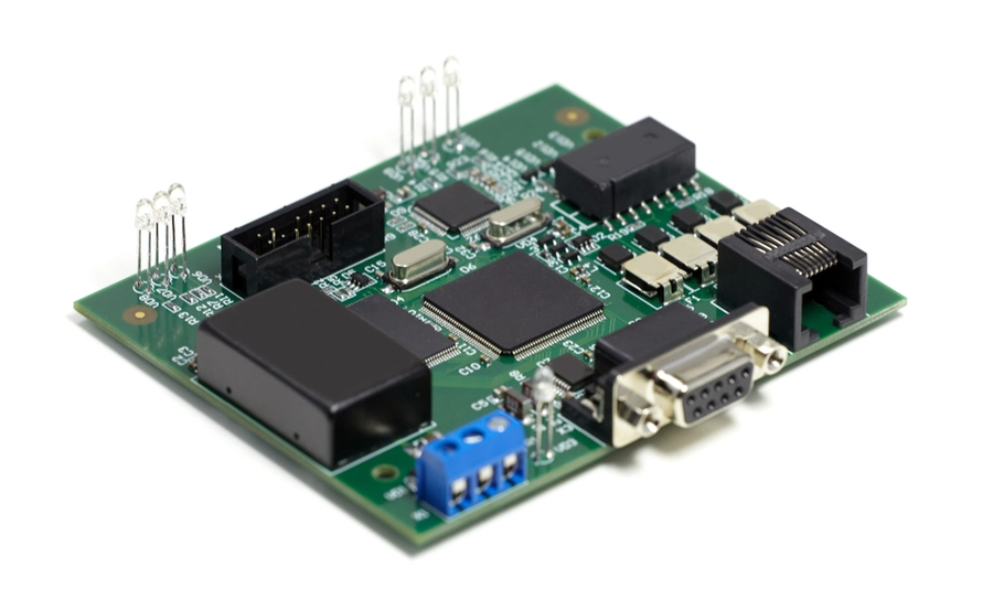
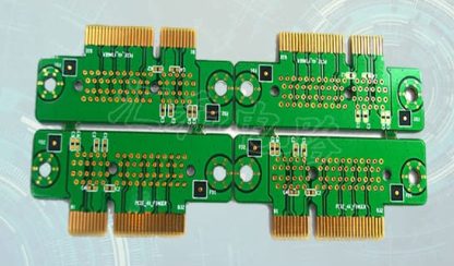
PCB design involves two critical stages: component layout and circuit connection wiring. The layout is the arrangement of circuit components within the PCB’s wiring area. A well-thought-out layout directly affects the ease of subsequent wiring and significantly impacts the PCB’s overall performance. In addition to meeting circuit functionality and performance requirements, a good layout considers manufacturability, inspection, and maintenance. Components should be placed evenly, neatly, and compactly, ensuring that leads and connections are short, minimizing interference and signal transmission delays.
Key Takeaways
The competitiveness of new product introduction makes it critical to optimize your prototype design process for effectiveness and efficiency.
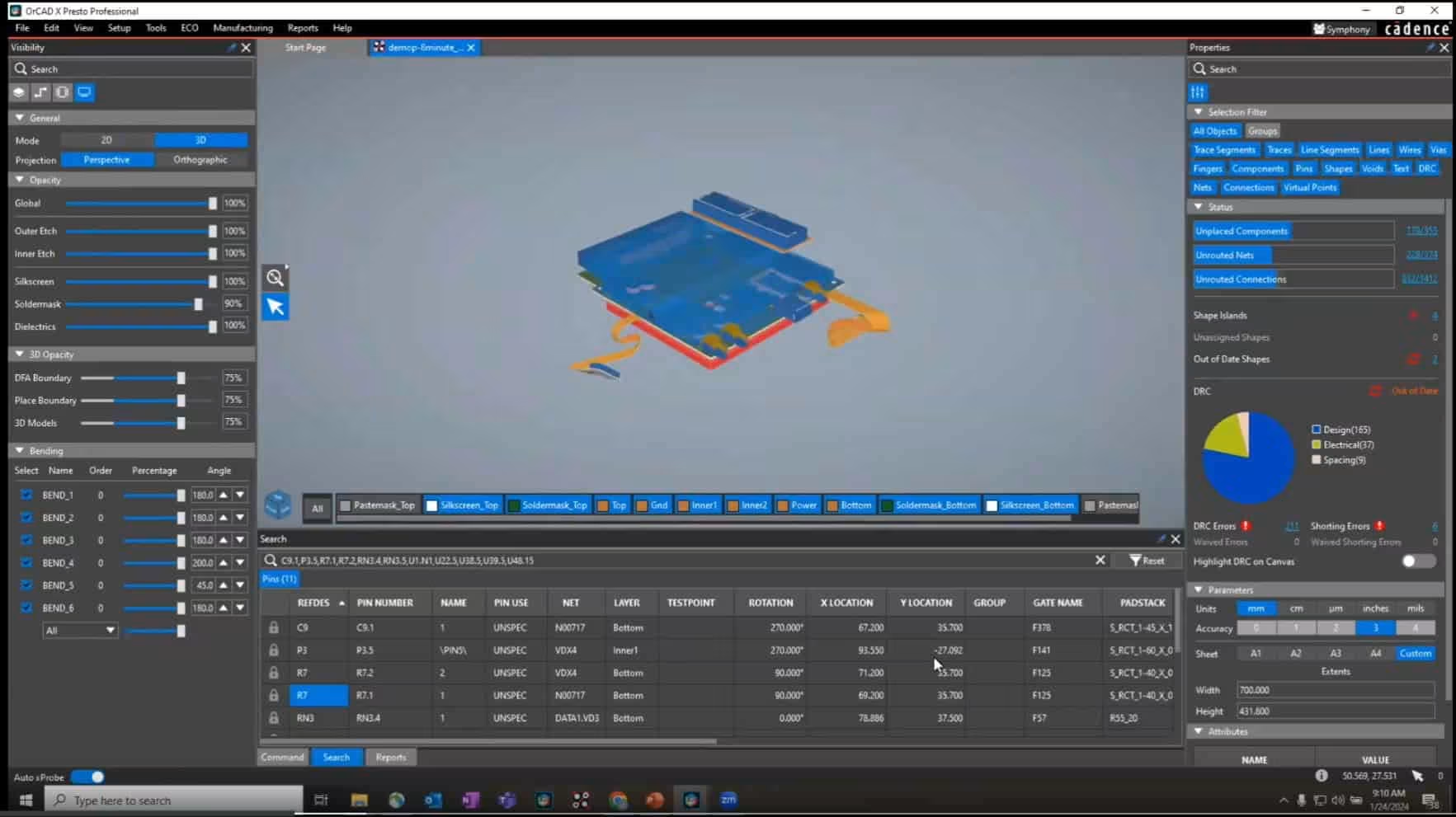
Your prototype PCB design software should exhibit essential attributes for managing component inventory, creating schematics, designing PCBs, verifying designs, and managing data.
OrCAD X delivers the essential functionality and capabilities in one program for prototype design optimization.
Key Takeaways
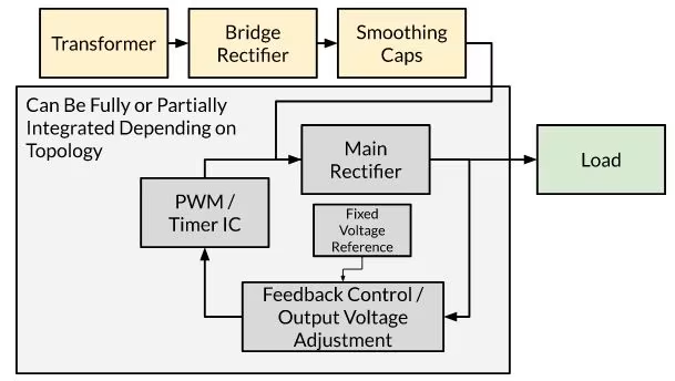
Understand the purpose of each component in a variable power supply, including transformers, rectifiers, capacitors, and regulators.
Learn about different topologies for variable power supplies, from discrete resistor selection to continuously variable potentiometer-based designs.
Discover how OrCAD X tools like DFM, interactive routing, constraint management, and thermal analysis can streamline the design and optimization of variable power supplies.
Key Takeaways
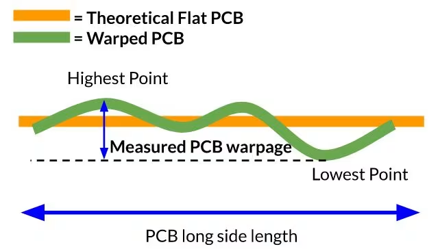
Stress during fabrication, such as thermal expansion and contraction, imbalanced copper distribution, and improper handling, can lead to warpage.
Utilize tools like feeler gauges, height gauges, contour gauges, optical profilometers, and Finite Element Method (FEM) simulations to accurately measure PCB warpage.
Effective design practices using OrCAD X, such as symmetrical component placement and proper copper distribution, combined with precise fabrication controls, can significantly reduce the risk of PCB warpage.
Maximize the efficiency of your design and manufacturing processes by optimizing your board development to mitigate the rigid flex PCB cost challenges
Key Takeaways
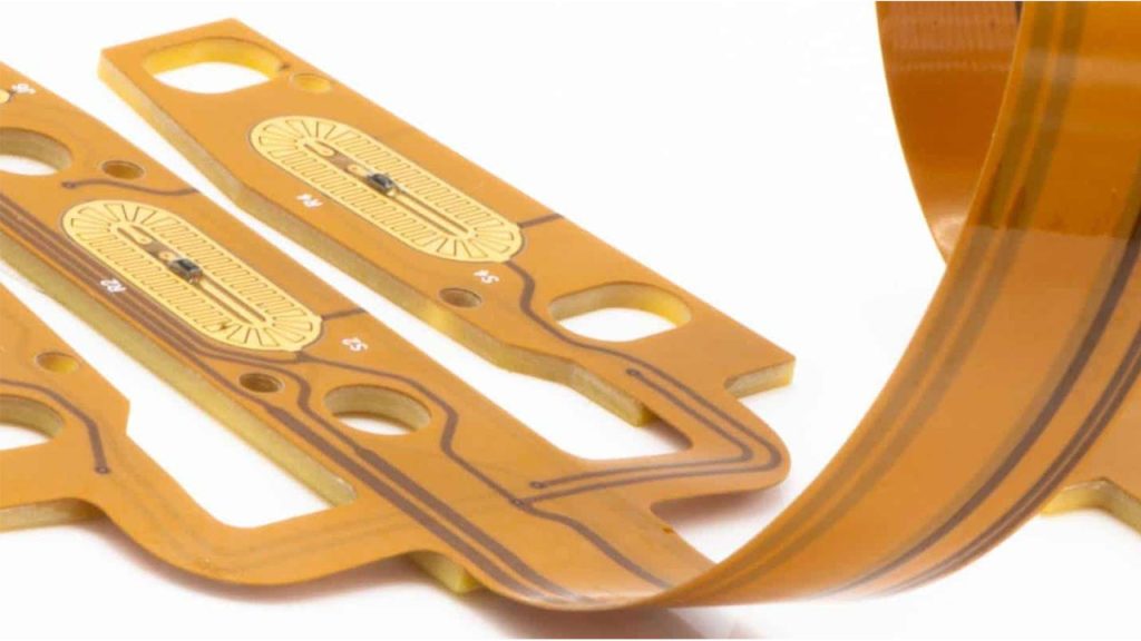
Cross-hatching significantly increases the flexibility of flex PCBs by reducing copper content.
Helps maintain optimal impedance in flex PCBs without altering dielectric thickness or signal line width.
Enables efficient manufacturing with reduced copper usage and improved resin adhesion.
Key Takeaways
Defining two major concepts of board design and production: class and build.
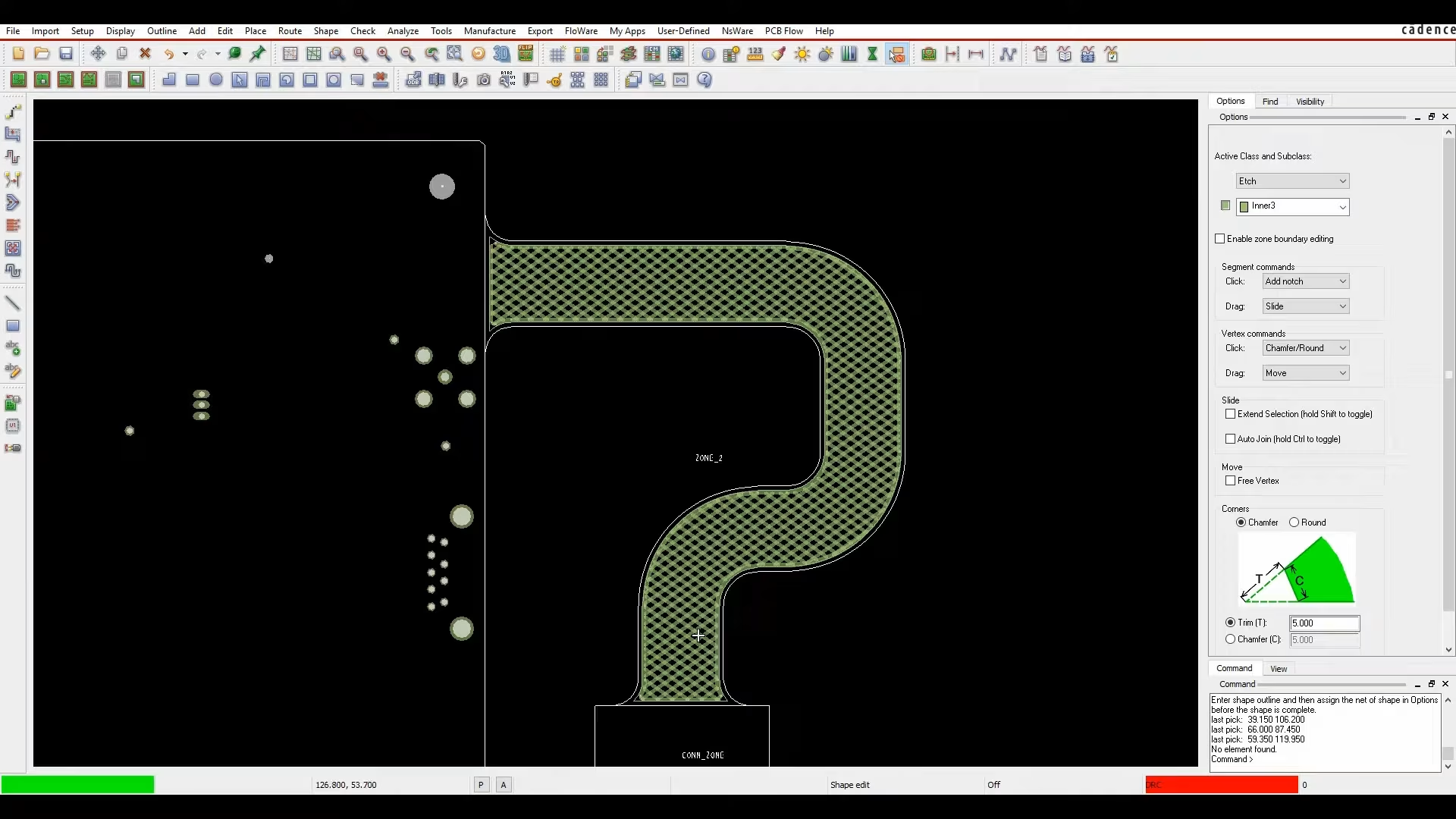
An overview of the layout department’s responsibilities: library part generation as well as placement and routing.
Stepping more granularly through each task from schematic/design document reception to manufacturing files.
This article starts with the most basic PCB layout and discusses the role and design techniques of PCB layer stacking in controlling EMI radiation