


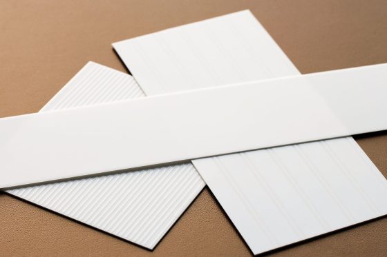
A wide range of glaze thicknesses, from 30μm to 200μm. Heat storage and heat dissipation can be controlled by adjusting the glaze thickness. Full-surface glaze or partial-surface glaze designs are available to suit application needs. Wet etching can be used to provide a variety of bump shapes and curvatures. Edge glazed substrates are also available.
The new NIKKO HTCC substrate uses platinum conductor, which is extremely chemically stable and not easy to oxidize, and can be used in various high-temperature environments.
Compatible with SDG, and does not require electroplating for surface treatment, which is low cost.
Bio-friendly material widely used in the medical field.
Provides the catalytic effect of Pt.
Compared with typical HTCC materials, it has higher strength due to the higher alumina content, while having the high thermal conductivity and low dielectric loss of ceramics.
High dimensional tolerance (±0.3%)
As sintering tool materials – high-purity alumina substrates with excellent surface flatness help improve the characteristics, quality and yield of sintered products. They are also ideal for sintering highly reactive materials. A variety of porosity levels are available due to the ability to control porosity during substrate sintering.
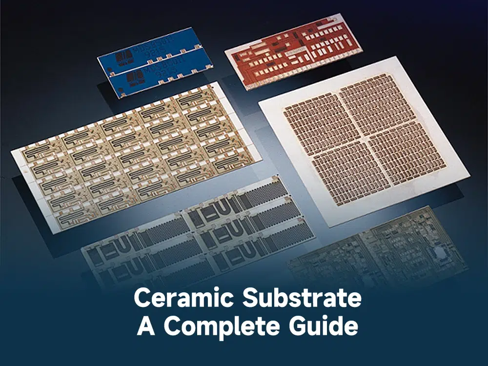
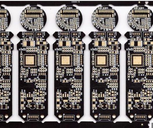
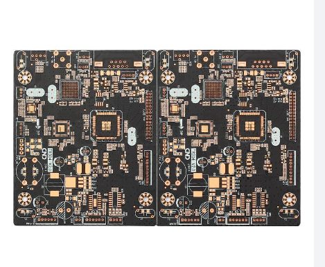
Shenzhen KKPCB Technology Co., Ltd. is a company that specializes in the design, manufacture, and assembly of various printed circuit boards (PCBs), including ceramic substrates.
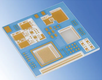
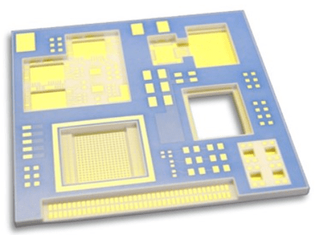
NIKKO LTCC substrates with silver conductor material provide multilayer substrates with low dielectric loss. Coils, capacitors and resistors can be embedded in the inner layer. Ideal for high-frequency modules and silicon wafer interposer substrates
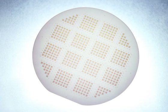
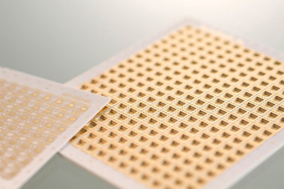
The thermal expansion coefficient of these LTCC substrates is adjusted for use as wafer-level packaging substrates. The substrate surface has bumps for electrical connections, and CSP (chip-scale package) can be easily assembled by directly bonding to silicon wafers. Ideal for MEMS and semiconductor ceramic packages with a small number of leads.
Low dielectric loss characteristics (tan δ) and low resistance conductors, low electrical loss, suitable for high-frequency applications
Due to our unique manufacturing technology, the size and characteristics of each production batch and within each batch vary little
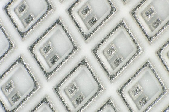
High-density wiring is achieved by improving stacking alignment accuracy
Precise control of substrate thickness and cavity shape
Resistance, inductance, and capacitance functions are built into the substrate and package
LTCC (Low Temperature Co-fired Ceramic) is a special type of ceramic material that integrates multiple ceramic layers together through a co-firing process. With its unique performance advantages, LTCC has found widespread application in circuits and systems operating at microwave, millimeter-wave, and higher frequencies.
With the rapid development of high-speed circuit design, PCB routing has evolved beyond simple interconnection tasks. Engineers must analyze various distributed parameters using transmission line theory. Distributed parameter circuits account for spatial variations in voltage and current. Modern PCBs, with their complexity and density, include advanced features like microvias, buried/blind vias, and embedded components (e.g., resistors, capacitors). These advancements require PCB designers to understand production processes deeply and adapt their designs to manufacturing constraints.
PCB design requires understanding physical processes and careful organization of layers, power networks, and signal paths. Following these recommendations reduces noise risk, improves reliability, and simplifies the routing of complex systems