


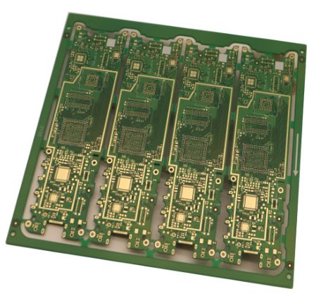
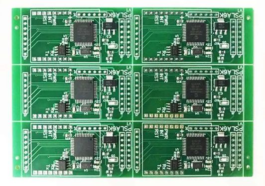
When designing high-speed PCBs, the layer stack-up plays a crucial role in ensuring signal integrity, minimizing crosstalk, and achieving optimal electromagnetic compatibility (EMC). For a standard six-layer board with a thickness of 1.6mm, selecting the right structure can significantly impact performance. Below is an analysis of common six-layer board structures and their suitability for high-speed designs
Impedance line routing in multi-layer PCBs is both an art and a science. Adhering to the principles of short lines, symmetry, equal length, and precise compensation ensures high-speed data transmission and robust device performance. By leveraging tools like the Polar Si9000 and applying best practices in design, engineers can effectively address challenges in modern PCB impedance routing.
Closely spaced vias are a common design challenge in multi-layer and high-speed PCB boards. Understanding the implications of tight spacing—such as drilling process inefficiencies, reduced solder ring size, and long-term reliability concerns—is essential. By adhering to recommended spacing guidelines, optimizing via placement, and collaborating with manufacturers, designers can enhance production yield, reduce costs, and ensure robust product per
In this context, ROGERS has introduced the RO4830™ material, which, with its excellent performance and lower cost, has become a key solution in driving the widespread adoption of 77 GHz millimeter-wave radar technology.
High-speed PCB design is crucial in fields like communication, computing, and graphics/image processing. Engineers in these areas often employ unique strategies tailored to their industry’s specific requirements. Below, we explore different approaches and key considerations for high-speed PCB design.
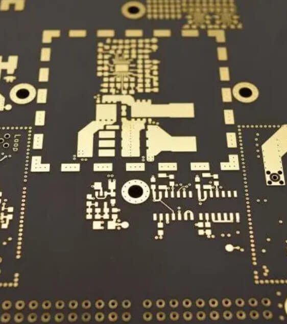
Solution Refinement and Layout: As the demand for smaller and more portable electronic devices continues to grow, the design of RF and microwave circuits is shifting towards more compact and efficient solutions. In high-frequency circuit design, the choice of PCB materials is crucial for determining circuit size, performance, and signal propagation characteristics. RT/duroid® 6010.2LM, a […]
Achieving efficient automatic PCB wiring involves a blend of strategic planning, tool utilization, and manual refinement. By setting robust design rules, optimizing layout, and leveraging EDA tools effectively, engineers can create high-quality PCB designs that meet performance and manufacturability requirements. The iterative approach of routing, validating, and refining ensures that even the most complex designs achieve high routing rates and functionality.
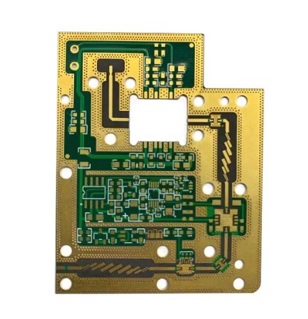
RF (Radio Frequency) circuits and interfaces exhibit unique characteristics, requiring specialized design considerations. These challenges are due to the nature of RF signals and their interaction with physical elements of the circuit. Understanding these aspects ensures optimal performance in wireless communication systems. Below is an exploration of RF circuit characteristics, PCB design considerations, and optimization techniques.
This guide delves into the four fundamental characteristics of RF circuits—RF interface, small desired signals, large interference signals, and adjacent channel interference—and highlights essential considerations for PCB design.
When designing high-speed PCBs, process variations and other factors can significantly impact actual impedance. Automated design tools may not always detect these subtleties, making proactive, defensive design essential. Here’s how to address common challenges in high-speed PCB design.