


When designing for PCB prototyping, the cost of individual parts does not always play a big role. If you’re designing one-offs or hobby projects, you’ll probably only look at parts prices when your assembly house sends you an invoice.
PCB edge plating is a specialized process that involves applying a metal coating to the exposed copper connections at the edge of a printed circuit board (PCB). This technique, also known as side plating, battlement, or metallized edge plating, enhances electrical connectivity, structural rigidity, and electromagnetic interference (EMI) shielding.
The Rogers RO4835 + IT180 hybrid PCB offers unparalleled performance for high-frequency and microwave applications, combining the best attributes of both materials. From automotive radar systems to advanced wireless communication and military-grade electronics, this hybrid PCB is optimized to meet the performance, durability, and reliability requirements of modern technologies.
The Rogers RO4835 + FR4 PCB material is a game-changer for 77GHz automotive millimeter-wave radar systems. Its stability, low loss, and superior performance at high frequencies make it the ideal choice for automotive applications such as ADAS, radar systems, and sensor modules.
A ceramic substrate is an insulating material that provides a stable and rigid platform for mounting electronic components and creating electrical circuits. Ceramic substrates are often used as an alternative to epoxy-based materials like FR-4 (Flame Retardant 4). FR-4 is a popular substrate material for PCBs, but ceramic substrates offer certain advantages in specific applications.
a PCB will operate in a high ambient temperature environment, and the board needs to remove heat from components to prevent even higher temperatures from being reached in the system. Active cooling measures are important for aiding heat flow, but not all products can accommodate active cooling. Instead, designs can rely on passive cooling that relies on choosing the right PCB materials.
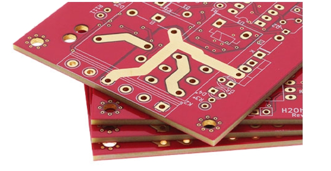
4-layer PCBs are the workhorses of many low-density digital and RF PCBs that still require some controlled impedance routing. 4-layer boards are also very useful for diverse power connections, and they can be used in power electronics that require many varied components and power levels.
Many times we discuss complex boards with unique features and sensitive routing on this blog. But the reality is that most PCBs that are mass manufactured have lower layer counts and less complexity. 2-layer boards will continue to be high-volume products, and they are almost always the starting point for a new designer learning about PCB layout.
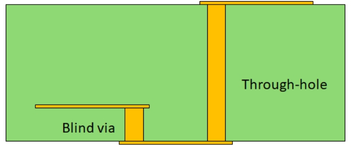
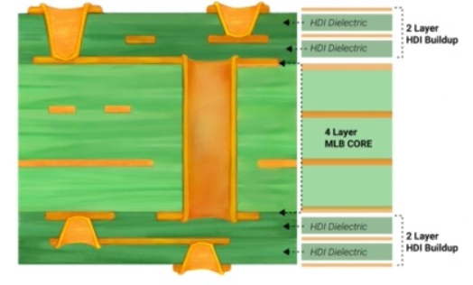
Fabrication capacity for high density PCBs and packaging is currently increasing, especially in North America and Europe. These platforms still use standard via styles, namely through-hole vias, blind and buried vias, and core vias in HDI PCBs. But the electronics assembly and packaging world is no stranger to innovation, and there are alternative via options that can offer much more flexibility in routing and layout.
One of the biggest design requirements in HDI PCBs is designing via stacks. Vias in an HDI PCB give you much more freedom than a standard board with through-hole vias, but the vias are also a big driver of manufacturing costs. These are also a big driver of reliability in the finished HDI build, especially when you look at challenges with stacked microvias.