


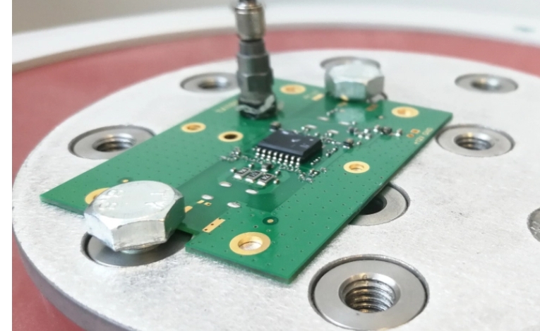
PCBs for commercial products must pass a set of reliability tests in order to prove their capabilities, which goes well beyond the standard functional testing found in many products. Functional tests are the starting point, but reliability tests are where a design is proven for operation in its intended environment. To help designers plan a path forward for reliability assessments, we have compiled a set of reliability tests for PCBAs.
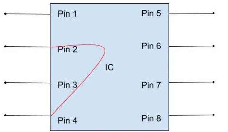
With the growth of the semiconductor industry, the density of circuits within integrated circuits (ICs) has increased. Even with the increase in density, the number of input-output pins remains unchanged, which is one of the reasons for the increased complexity in IC packages.
Ceramics used in electronics are everywhere. For instance, ferroelectrics are used to create high-dielectric capacitors and non-volatile memory devices. Ferrites play a crucial role in storing data and information. Solid electrolytes are instrumental in the storage and conversion of energy. Piezoelectrics are essential for sonar technology, while semiconducting oxides have been pivotal in monitoring environmental conditions.
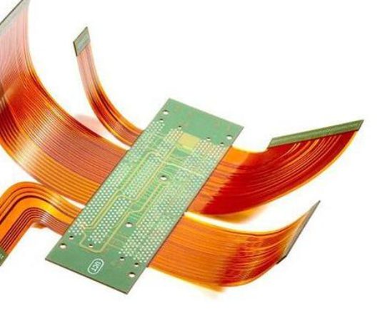
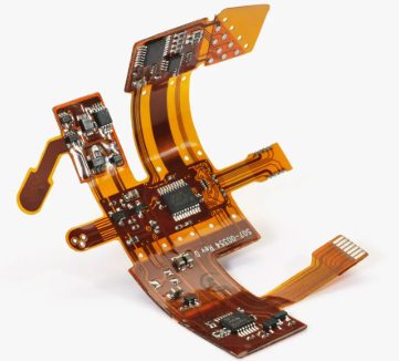
Rigid-flex PCBs represent a groundbreaking advancement in electronics design, combining the best features of rigid boards and flexible circuits. By integrating high-density interconnect (HDI) technology, rigid-flex PCBs eliminate the need for traditional board-to-board connectors and simplify assembly processes.
As the demand for flexible and rigid-flex PCBs continues to grow, understanding the factors that influence their cost is crucial for optimizing designs and ensuring cost-effective production. Rigid-flex PCBs offer significant advantages, such as enhanced flexibility, reliability, and space-saving capabilities, but they also come with unique challenges that can drive up costs if not properly managed. This article explores key design considerations, cost factors, and strategies for optimizing rigid-flex PCB designs.
High-density interconnect (HDI) PCBs have become a standard in modern electronics, enabling designers to create smaller, more functional devices. However, designing HDI PCBs requires careful attention to detail due to their complexity and the advanced technologies involved. This article outlines key HDI PCB design guidelines, highlights the advantages and disadvantages of HDI layouts, and provides insights into overcoming common challenges.
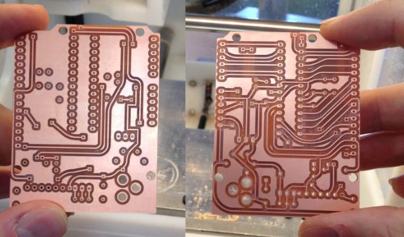
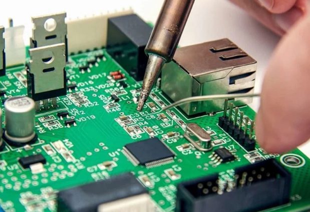
Troubleshooting printed circuit boards (PCBs) can be a daunting task, but with a systematic approach, it becomes manageable and efficient. This guide provides a step-by-step process to identify faulty components on PCBs, along with methods tailored to specific component types and advanced techniques for batch inspection.
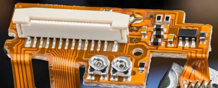
As the demand for more compact, reliable, and flexible electronic devices grows, rigid-flex PCBs are becoming increasingly popular. These boards combine the best of both rigid and flexible circuits, offering unique advantages such as enhanced durability, reduced package size, and fewer connectors.
Designing double-sided PCBs requires careful planning to ensure efficient assembly, high yields, and reliable solder joints. Solder paste application and stencil design play a critical role in achieving these goals. This article explores key considerations for solder paste and stencil design, focusing on double-sided PCBs, component orientation, and advanced techniques for fine-pitch devices.
When designing a printed circuit board (PCB), engineers often focus on ensuring the correct impedance structures and electrical performance of the board. However, the physical characteristics, such as PCB thickness, are equally important and can significantly impact the cost, manufacturability, and performance of the final product. While standard PCB thicknesses are widely used, they are more of a convention than a strict requirement, offering designers an opportunity for optimization, especially in high-volume production.