


The primary challenge of this project was ensuring that the high-frequency PCB maintained extremely low attenuation and distortion during signal transmission while preventing external interference from affecting signal quality.
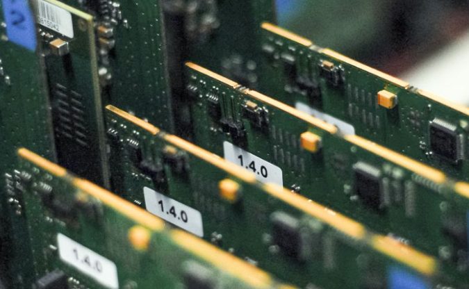
kups is one of the most critical aspects of HDI PCB design. Vias in HDI PCBs offer greater flexibility compared to standard boards, but they also significantly impact manufacturing costs and reliability.
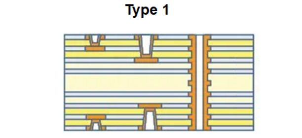
As high-density interconnect (HDI) designs with larger layer counts become more prevalent, the use of microvias is increasing. In builds with 3+N+3 or larger configurations, sequential lamination now often relies on skipped vias, staggered microvias, and stacked microvias
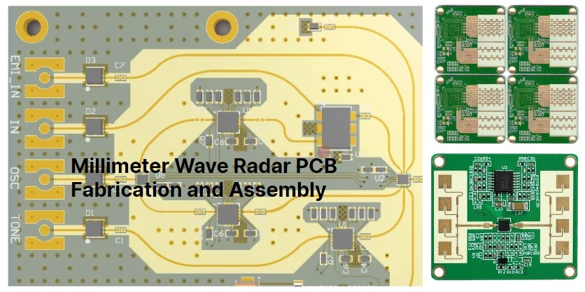
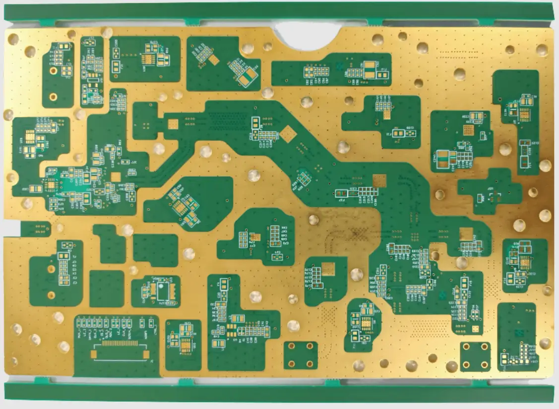
PCB Processing The precise dimensions required for millimeter-wave circuits demand well-controlled PCB processing techniques to produce circuits with consistently excellent performance. Variations in copper plating thickness and final surface treatment on the conductor surface can impact the performance of millimeter-wave circuits. To ensure the successful fabrication of high-performance millimeter-wave circuits, both of these processes must […]
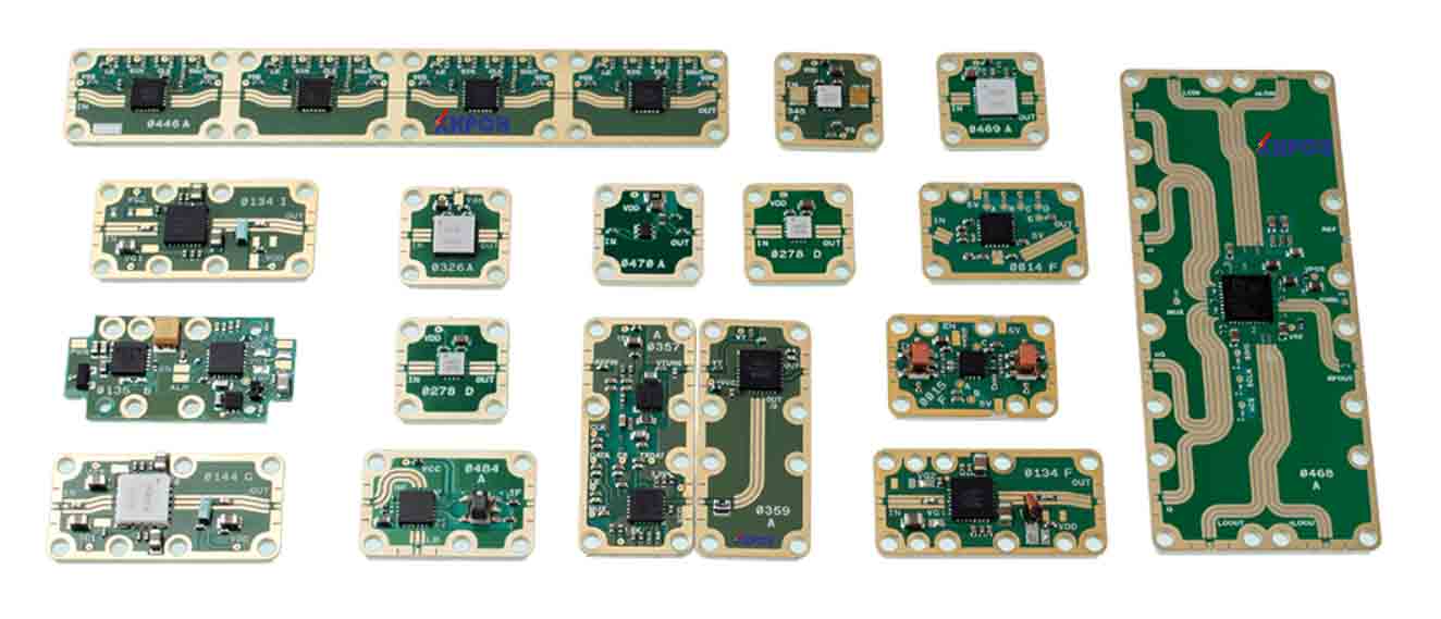
From anti-collision radar systems used in autonomous vehicles to the fifth-generation (5G) high data rate New Radio (NR) networks, the application of millimeter-wave (mmWave) circuits is growing rapidly. Many applications are pushing the operating frequency bands to higher frequencies (such as >24GHz).
Printed Circuit Boards (PCBs) are a fundamental component in electrical engineering. They are used to create electronic circuits by arranging components such as transistors and resistors on a copper-based wiring pattern on the surface of an insulator (typically plastic) and then soldering them.
RO4000® hydrocarbon ceramic laminates are designed to off er superior high frequency performance and low cost circuit fabrication. The result is a low loss material which can be fabricated using standard epoxy/glass (FR-4) processes off ered at competitive prices. The selection of laminates typically available to designers is signifi cantly reduced once operational frequencies increase […]
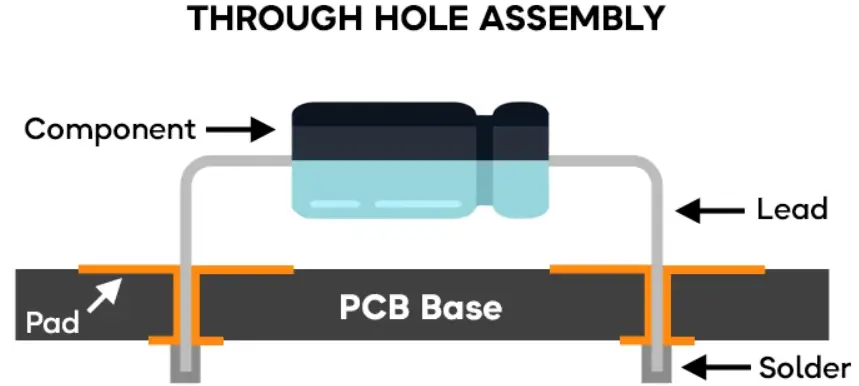
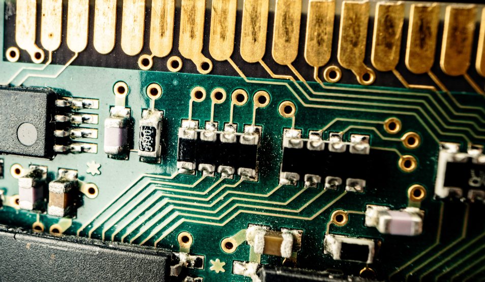
One of the two most common methods of attaching electronic components to PCBs is the through-hole or through-hole process. This technology is older than SMT, and for many years, it was the standard technology for PCB assembly. When surface mount technology became popular in the 1980s, many people thought it would make through-hole PCB assembly obsolete. However, through-hole technology has several advantages that make it still a preferred choice for certain applications.
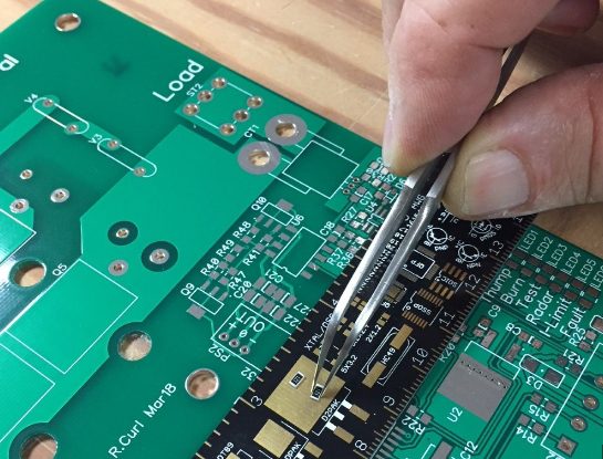
Basic soldering guide on how to solder electronic components to a printed circuit board (PCB). This is a detailed and complete soldering guide for both automated soldering in mass production and manual soldering in PCB rework and repair.
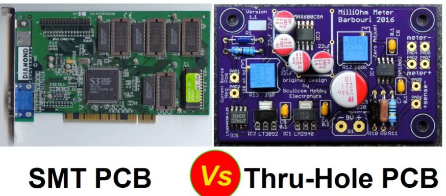
SMT vs. Through-Hole – Disadvantages of SMT vs. Through-Hole
Since not all basic electronic components are available for surface mounting, the actual area savings on the board will depend on the percentage of through-hole components replaced by surface mount components. The three types of surface mount offer varying degrees of benefit depending on the component combination.