


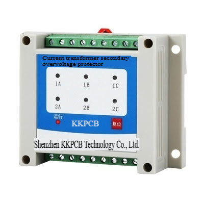
Current Transformer PCBA Solution for Industrial Automation
1. Background Overview
A European industrial customer focusing on smart distribution systems required a highly accurate, low-loss, and production-friendly current transformer PCBA. The solution needed to integrate current sensing, energy monitoring, and protection features while maintaining cost-effectiveness and production scalability.
2. Application Scenario
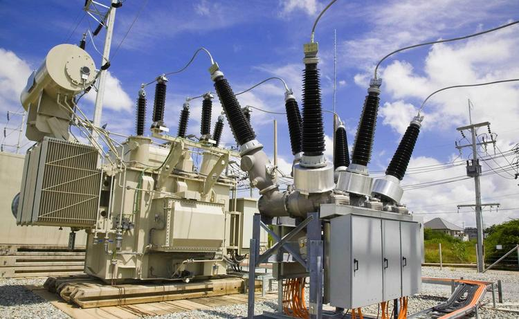
The PCBA is integrated into smart distribution cabinets, serving as the core module for real-time current monitoring across high and low voltage circuits. It supports load distribution, power quality analysis, and abnormality diagnostics. Key use cases include smart factories, intelligent building energy systems, and data center power management.
3. Product Specifications
| Item | Specification |
|---|---|
| Current Range | 5A ~ 200A |
| Accuracy Class | 0.5 Class |
| Output Signal | Analog Voltage 0–5V / Current 4–20mA |
| Operating Temperature | -25°C to +85°C |
| Mounting Method | Through-hole on PCB |
| Electrical Isolation | ≥2.5kV |
| PCB Dimensions | 45mm x 32mm |
| Operating Voltage | DC 5V / 12V optional |
4. Results of Implementation
- Quality: PCBA pass rate increased to 99.8% with improved soldering reliability.
- Cost: BOM cost reduced by 12% through layout and component optimization.
- Performance: Signal drift decreased to ±0.1% with enhanced EMC shielding.
- Delivery: Lead time reduced to under 15 working days using a streamlined process.
5. KKPCB Advantages Highlighted in This Case
KKPCB brings extensive experience in power monitoring, industrial control, and sensor-based PCBA manufacturing. From Gerber evaluation to DFM (Design for Manufacturability) reviews, we ensure every board meets IPC-A-610E standards. Our dual-line SMT and DIP processes support both high-reliability and low-to-medium volume production. We also provide complete ICT/FCT testing solutions and full traceability with barcoding integration.
6. KKPCB’s Custom Manufacturing Solution
For this project, KKPCB delivered a tailored PCBA manufacturing solution:
- PCB Optimization: Designed a dual-layer board with isolated signal zones to boost measurement precision.
- Component Layout Improvement: Rearranged high-voltage components to improve EMC and ease assembly.
- SMT + DIP Workflow: Used a fully automated hybrid production line to ensure high consistency.
- Custom Testing Fixtures: Built in-line current simulation and full-load aging testing for 100% pre-shipment validation.
- Board-Level Traceability: Enabled full MES integration with barcode tracking for each PCBA unit.
7. Real-World Performance Outcomes
After deploying KKPCB’s solution, the customer cut lead times from 20 to 12 working days, alleviating seasonal delivery pressure. Current measurement accuracy improved from ±1.2% to ±0.3%, enhancing final product competitiveness. The PCBA batch yield stabilized above 99.8% with optimized process flow and testing systems, earning positive feedback on quality, efficiency, and responsiveness.