


Customized PCBA Solution for Industrial Smart Sensor
1. Background Overview
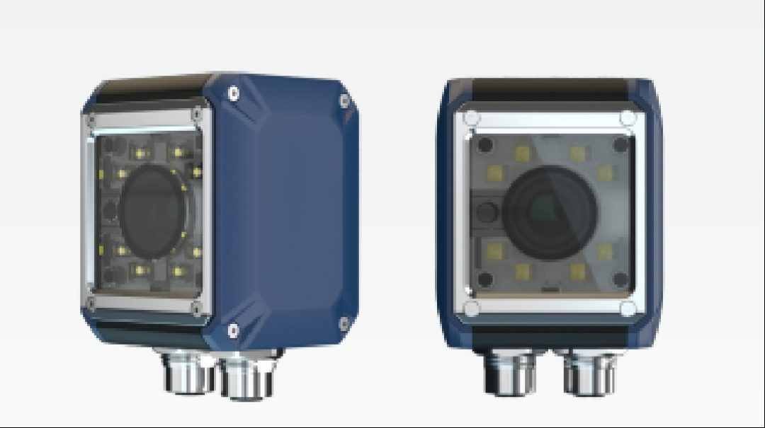
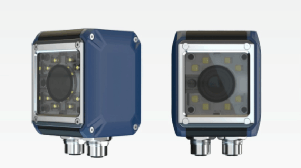
A European client aimed to develop a high-performance industrial smart sensor for industrial automation systems. The device needed to be compact, highly reliable, and compatible with multiple sensor types, while supporting robust communication protocols and protection mechanisms. To meet their high reliability and mass production consistency requirements, the client partnered with KKPCB for end-to-end PCB manufacturing and PCBA assembly solutions.
2. Application Scenarios
This industrial smart sensor is widely applied in:
- Industrial equipment condition monitoring
- Automated production line control
- Smart manufacturing systems
- Energy management and supervision
- Industrial IoT (IIoT) environments

3. Product Specifications
| Specification | Details |
|---|---|
| Input Voltage | DC 3.3V – 5V |
| Communication | RS485 / Modbus RTU / BLE |
| Sensor Compatibility | Temperature, Humidity, Pressure, Vibration |
| Operating Temperature | -40°C to +85°C |
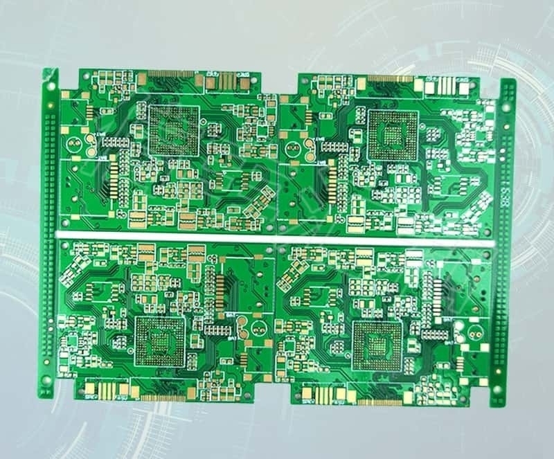
| PCB Size | 50mm × 40mm, 4-layer board |
| Certifications | RoHS / CE / EN61000 |
4. Application Results
With KKPCB’s advanced manufacturing solution, the client achieved:
- ✅ First-pass yield of 99.7%, 2.2% higher than their previous supplier
- ✅ 18% reduction in PCBA cost, thanks to optimized processes and component alternatives
- ✅ 25% lead time improvement, cut from 20 working days to 15
- ✅ 15% increase in sensor data accuracy, with more stable control responses
- ✅ Outstanding thermal reliability, with zero failures after 1000+ hours of thermal cycling
5. KKPCB Advantages Demonstrated in This Project
In this project, KKPCB delivered value through:
- Mature multilayer board manufacturing with impedance control and thermal design
- High-density SMT capabilities suitable for compact, high-precision sensor components
- Complete inspection system (AOI/ICT/functional testing) to reduce rework rates
- Flexible small-batch & quick-turn services, ideal for fast iteration cycles
- Strong local sourcing network, reducing BOM cost and improving material lead time
6. Manufacturing-Focused Customized Solution (PCB & PCBA Level)
To address early-stage challenges like thermal performance and EMI, KKPCB proposed and implemented the following:
- PCB structure and thermal design optimization: 4-layer board with adjusted power/ground planes to improve EMC and heat dissipation
- Thicker copper tracks (2oz) in power areas to handle high current and enhance heat management
- Component layout refinement to isolate analog and digital zones, reducing interference
- Custom reflow profiles tailored for mixed-pitch components and sensitive ICs
- Selective potting to improve vibration resistance in critical areas
7. Real-World Impact
The customized solution achieved significant improvements in the client’s production:
- Quality: Verified by X-Ray and thermal shock testing, in-field failure rate dropped below 0.1%
- Cost: 18% overall PCBA cost reduction through panelization and local sourcing strategies
- Performance: Enhanced EMI protection and thermal stability led to improved sensing accuracy
- Lead Time: KKPCB’s flexible production scheduling reduced lead time from 20 to 15 working days, helping the client accelerate product launch