


Industrial Ethernet Switch PCBA Solution Case Study
1. Background
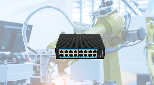
As industrial automation continues to evolve, a European client sought to develop a rugged, high-performance industrial Ethernet switch capable of operating in harsh environments with excellent anti-interference capability. The client required a reliable PCBA partner to meet strict demands in product quality, electromagnetic compatibility (EMC), and delivery schedule.
KKPCB was selected as the manufacturing partner thanks to its solid experience, certified quality system, and rapid response, delivering a tailored solution for PCBA manufacturing and assembly of the industrial switch.
2. Application Scenarios
The industrial Ethernet switch is widely used in various industrial networking applications:
- Smart manufacturing production lines
- Data acquisition and remote control in power systems
- Signal transmission in railway transportation
- Device-to-device communication in factory automation
- Streetlight control and monitoring in smart cities
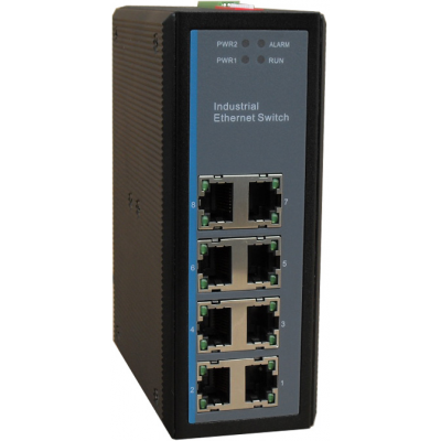
3. Key Product Specifications
| Specification | Value |
|---|---|
| Operating Voltage | DC 12~57V |
| Network Ports | 5 × 10/100/1000 Mbps RJ45 auto-adapt |
| Port Protection | 4KV lightning protection per port |
| EMC Rating | IEC61000-4-5/4/3/4/2/6 compliant |
| Enclosure Material | Metal casing |
| Operating Temperature | -40°C to +85°C |
| Mounting | DIN rail mounting |
| Power Connector | Terminal block |
| Power Consumption | < 5W |
4. Outcome of the Application
With KKPCB’s support, the client successfully launched mass production of the Ethernet switch PCBA and applied it to multiple industrial projects. Highlights include:
- Product yield rate reached 99.95%, ensuring long-term stability
- EMC performance improved by over 30%, with first-pass EMC certification
- Production lead time reduced to 14 calendar days, ~20% faster than the industry average
- Post-assembly performance stability improved, with a field return rate under 0.2%
- Manufacturing cost lowered by approximately 8%, due to BOM optimization and efficient production
5. KKPCB Advantages Highlighted in This Case
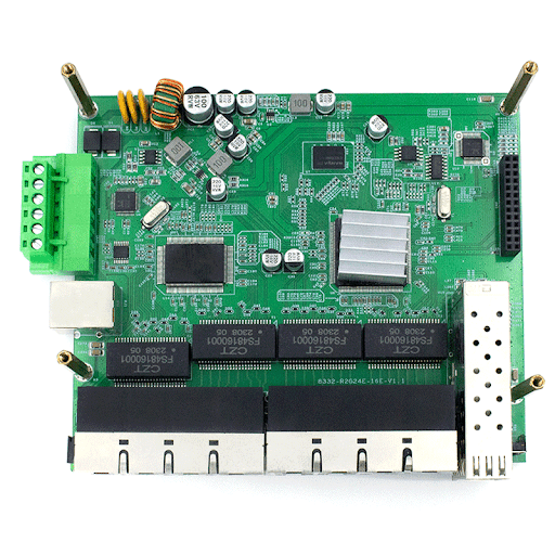
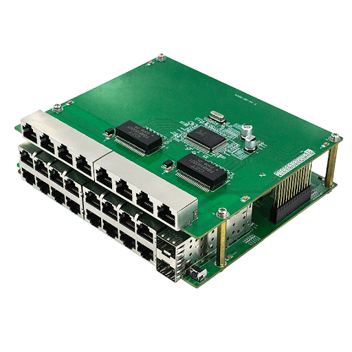
KKPCB demonstrated its advanced capabilities in high-speed multilayer PCB fabrication—ensuring signal integrity and superior EMC performance. Our rigorous PCBA processes and comprehensive SMT + through-hole + testing workflows guaranteed reliable assembly and functionality.
The engineering team provided real-time support and design-for-manufacturing (DFM) consultation, enabling smooth coordination from prototyping to mass production. KKPCB also offered valuable experience in compliance with European EMC and CE regulations, which helped the customer pass testing efficiently.
6. KKPCB’s Custom Manufacturing-Focused Solution
Focusing on PCB manufacturing and PCBA assembly, KKPCB tailored the following solution:
- For PCB fabrication, we proposed a 6-layer stack-up with low-loss materials optimized for high-speed signal transmission, meeting both impedance control and EMC requirements.
- For PCBA assembly, a dedicated production line for industrial communication products was established, including AOI, X-ray inspection, and high-temperature aging tests.
- Static-sensitive and surge-prone components were shielded with optimized ESD layout and protective devices.
- We proactively refined the BOM structure—recommending cost-effective, quality-guaranteed substitutes—resulting in a better price-performance ratio.
- To support the client’s project timeline, we enabled flexible delivery strategies with bilingual documentation and technical support.
7. Results Achieved
The customized manufacturing solution led to measurable improvements:
- Stability: Switch units ran continuously for 60 days at -40°C to +80°C without failure
- EMC Compliance: Successfully passed EMI/EMS pre-certification for CE
- Cost Reduction: ~8% decrease in manufacturing cost via layout and BOM optimizations
- Lead Time: Prototype delivered in 3 weeks; batch production within 14 days
- Defect Rate: Post-deployment return rate kept below 0.2%, outperforming industry norms