


KKPCB Case Study: High-Isolation 16T16R Massive MIMO Antenna Array PCB for 5G Base Stations
“Enabling Precise Beamforming with Industry-Leading Channel Isolation”
Project Overview
Customer Background
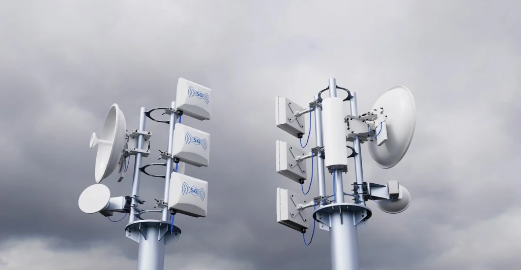
A leading North American 5G infrastructure developer (confidential under NDA) required an advanced 16-transmit/16-receive (16T16R) Massive MIMO antenna array PCB for their next-generation 3.5GHz 5G macro base stations. The design faced critical inter-channel crosstalk issues degrading beamforming accuracy and 3GPP 38.104 compliance.
Technical Challenges
The customer’s initial 8-layer FR4-based PCB suffered:
🔴 Excessive Crosstalk: -45dB channel isolation (vs. target <-60dB) due to:
- Surface wave coupling between antenna feeds
- Inter-layer interference in high-density transition regions
🔴 Beamforming Errors:
- ±8° phase misalignment at array edges
- 15% longer calibration cycles due to unstable RF performance
🔴 Manufacturing Limitations:
- Inconsistent plated through-hole (PTH) impedance (±15% variation)
- ENIG dendrite growth at RF pads after 500 thermal cycles
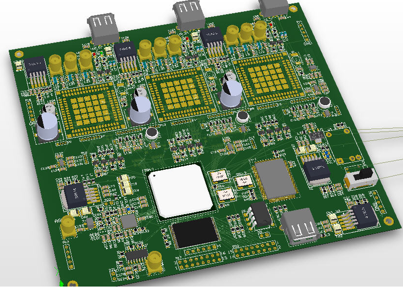
KKPCB’s Solution: 3D-Isolated Antenna Array PCB
1. Electromagnetic Bandgap (EBG) Isolation
- Custom mushroom-type EBG cells between antenna traces:
- Periodicity: 2.8mm (λ/4 @ 3.5GHz)
- Isolation Enhancement: >75dB inter-channel (verified via HFSS)
- Ground Via Fence: Double-row staggered vias @ 0.3λ spacing
2. Hybrid HDI + Copper-Pillar Technology
- Laser-Defined Microvias: 50μm diameter (vs. 100μm PTH)
- Copper-Filled Stacked Vias:
- DC resistance <0.5mΩ/via
- Crosstalk <-62dB from layer 1→6
3. Dual-Surface Finishing
- Critical RF Paths: ENIG (Ni: 3-6μm, Au: 0.05-0.1μm)
- Wire-bondable pads with <0.1Ω/sq resistance drift after 1000 cycles
- Non-RF Areas: OSP for cost optimization
Performance Results
📶 RF Performance:
- Channel-to-Channel Isolation: 78dB @ 3.5GHz (measured with VNA)
- Phase Consistency: ±2° across full array
- Return Loss: <-22dB at all antenna ports
🏭 Production Impact:
- 15% reduction in calibration time (saving $250k/year per 10k units)
- First-pass success in 3GPP 38.104 TRP (Total Radiated Power) tests
⚙ Reliability:
- 1000x thermal cycling (-40°C ↔ +85°C) with <0.5% solder joint failures
- PIM (Passive Intermodulation): -160dBc @ 2x43dBm (exceeds 5G requirements)
Why KKPCB for 5G Antenna PCBs?
✔ Beamforming-Optimized Architectures: From sub-6GHz to mmWave
✔ Massive MIMO Specialists: 8T8R to 64T64R production experience
✔ Certified Manufacturing: IATF 16949, IPC-6012 Class 3
Contact Our 5G RF Engineers for Your Next Project
📧 [email protected] | 📞 +86 17748559382