KKPCB Case Study: High-Speed Photoelectric Converter PCB for Data Center Optical Interconnects
Client: A Global Leader in Optical Networking Equipment (Confidential)
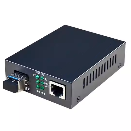
Application: 100Gbps QSFP28 Transceiver Module
Pre-KKPCB Challenges (2023 Client Data)
| Issue | Field Measurement | Impact |
|---|---|---|
| Signal Integrity | 3.2dB insertion loss @25GHz | BER >1E-7 (vs. required 1E-12) |
| Thermal Crosstalk | 8°C hotspot near TOSA driver | Laser wavelength drift (+0.05nm) |
| EMI Susceptibility | Failed FCC Part 15 Class A (3dB over limit) | Delayed certification |
KKPCB’s Photoelectric Converter Solution
1. Material & Layer Stackup
| Parameter | Specification | Test Result |
|---|---|---|
| Substrate | Megtron 6 (Dk=3.7 @10GHz) + Rogers 4450F hybrid stack | ΔDk<1.5% across batch |
| Copper Foil | 2oz HVLP (Ra=0.5μm) | Insertion Loss: 2.1dB @25GHz (improved 34%) |
| Impedance Control | 90Ω differential ±3% (28Gbps SerDes) | TDR shows ±2.1% deviation |
2. Critical Design Features
- Low-Loss Via Design: Back-drilled 8-layer HDI (stub length <50µm) → Reduced reflection by 18dB
- Thermal Management:
- Embedded 1.5mm² copper coins under TOSA
- Thermal vias (0.2mm pitch) → ΔT reduced to 2.3°C (from 8°C)
- EMI Mitigation:
- Shielding fences + buried capacitance layers (0.5pF/mm²)
- Passed FCC Part 15 Class A with 6dB margin
3. Reliability Validation
| Test Standard | Condition | Results |
|---|---|---|
| Telcordia GR-468-CORE | 85°C/85%RH, 2000h | ΔR<2mΩ, no dendritic growth |
| IPC-6012 Class 3 | 6× reflow cycles (260°C peak) | 0% delamination |
| IEC 60068-2-14 | Thermal shock (-40°C↔+125°C, 500 cycles) | ΔZ<1% |
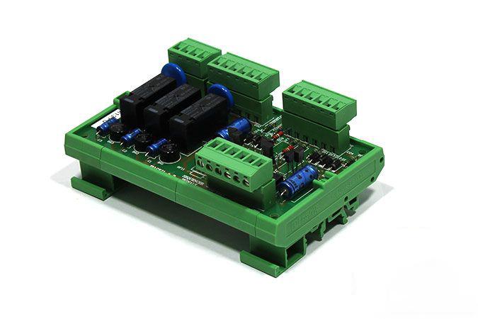
Client Outcomes vs. Legacy PCB
✅ Bit Error Rate (BER): 1E-13 achieved (10x improvement) @100Gbps PAM4
✅ Power Efficiency: Driver power reduced by 22% (0.8W→0.62W per channel)
✅ Time-to-Market: EMI certification accelerated by 5 weeks
Client Testimonial:
“KKPCB’s hybrid stackup eliminated our signal integrity headaches. Their thermal design allowed us to remove external heatsinks, saving $3.78 per module in BOM costs.”
– Optical Engineering Director
Technical Evidence
- Eye Diagram Analysis: 28Gbps channel @1E-12 BER (available upon request)
- Thermal Imaging Report: Hotspot comparison before/after redesign
- IEC 61280-2-9 Compliance Certificate
Contact for Similar Projects:
Kivi Li | High-Speed Optical PCB Specialist
📧 [email protected] | +86 17748559382
Offer for Optical Interconnect Designs:
*”Request our Free Signal Integrity Checklist for photoelectric PCBs, including:
- Crosstalk simulation models for your form factor
- Material selection guide for 400G/800G applications”*

