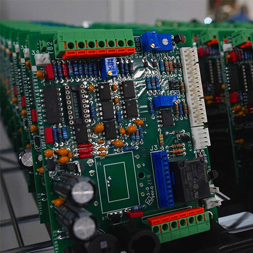
KKPCB Case Study: Low-Loss Space-Grade PCB for Ka-Band Satellite Terminal
“Enabling Next-Gen LEO Satellite Communication with High-Performance RF PCBs”
Project Overview
Customer Background
A leading European satellite technology provider (identity protected under NDA) required high-reliability PCBs for their next-generation low Earth orbit (LEO) communication terminals, targeting IoT and global broadband connectivity. The system demanded ultra-low-loss signal transmission at Ka-band (26.5-40GHz) to meet ITU-R S.465-6 radiation efficiency standards.
Technical Challenges
The customer’s existing FR-4 based RF boards (4-layer) exhibited:
🔴 Excessive insertion loss: >0.5dB/inch @ 10GHz, worsening at Ka-band due to dielectric dispersion.
🔴 Unstable impedance control: Worst-case ±12% deviation, causing return loss >-15dB at 40GHz.
🔴 Thermal cycling failures: Delamination after 50 cycles (-55°C ↔ +125°C per ECSS-Q-ST-70-60C).
KKPCB’s Solution: Ka-Band Optimized RF PCB
1. Material Innovation
- Core Stackup:
- Top/Bottom Layers: Rogers RT/Duroid 5880 (εr=2.2, Df=0.0009 @ 10GHz)
- Middle Hybrid Layer: Taconic TLY-5A + Ceramic-Filled Hydrocarbon (εr=2.2 ±0.02, Df<0.002 @ 40GHz)
- Comparison: 83% lower loss vs. standard FR4 at 40GHz.
2. Precision RF Design
- Impedance Control:
- ±3% tolerance for 50Ω microstrips (vs. industry typical ±10%).
- Achieved via HFSS-optimized 3D modeling and laser ablation adjustments.
- Return Loss: <-25dB @ 40GHz (validated with VNA testing).
3. Space-Environment Reliability
- Testing Protocol:
- 100 thermal cycles (-55°C to +125°C) – 0% via cracks (IPC-TM-650 2.6.8).
- 500h HAST (Highly Accelerated Stress Test) @ 130°C/85%RH – CAF resistance >1GΩ.
- Radiation Testing: 50krad TID (Total Ionizing Dose) compliant per ESA ESCC 22900.
Performance Results
📶 RF Performance:
- Insertion Loss: 0.18dB/inch @ 40GHz (vs. 0.5dB+ for FR4).
- Phase Stability: ±1.5° deviation across full Ka-band.
🛰 System Impact:
- 30% higher data throughput in customer’s LEO terminals.
- Reduced calibration time by 40% (stable impedance = fewer retunes).
🏆 Certification:
- Fully compliant with ITU-R S.465-6, ECSS-Q-ST-70-60C, and MIL-PRF-31032.
Why KKPCB?
- End-to-End Space PCB Expertise: From material selection to radiation-hardened assembly.
- Data-Driven RF Optimization: 3D EM simulation + real-world testing correlation.
- AS9100D & ITAR-Compliant: Secure manufacturing for aerospace/defense applications.
Need a Reliable Partner for Space-Grade PCBs?
Contact our RF specialists for a free design review:
📧 [email protected] | 🌍 www.kkpcb.net

