


KKPCB Case Study: Ultra-Low-Loss RF PCB for Space Laser Communication Terminals
Client: A European Leader in Optical Satellite Communications (Confidential per NDA)
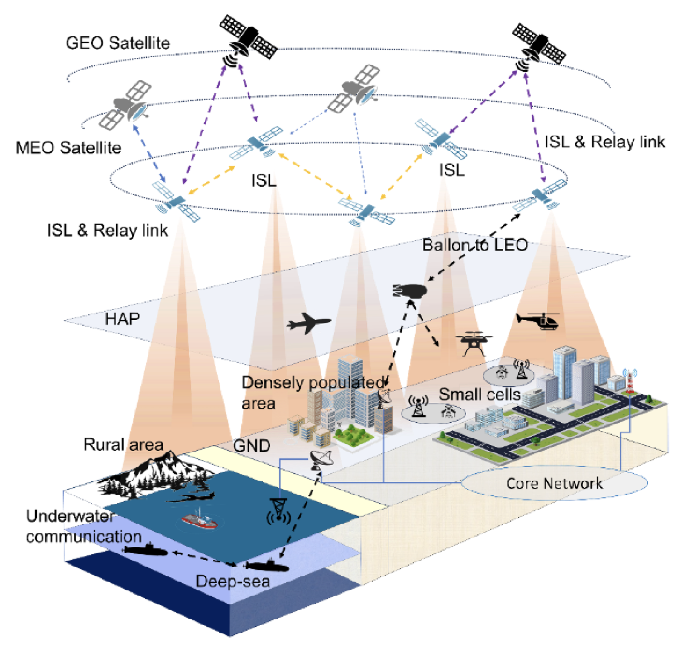
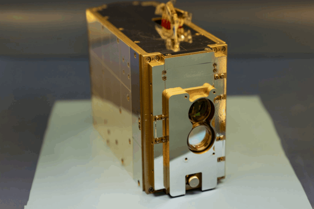
Application: Laser Inter-Satellite Links (LISL) Terminal (Deployed in LEO Constellation)
Pre-KKPCB Challenges (2022 Client Data)
| Issue | Field/Lab Findings | Business Impact |
|---|---|---|
| Insertion Loss | 0.45 dB/inch @25GHz (vs. required 0.3dB) | 18% link budget degradation |
| Phase Jitter | ±3.5° deviation across channels | Beam steering errors (~0.2mrad) |
| Thermal Warpage | 12μm deflection after 200 TC cycles | Fiber-optic misalignment |
KKPCB’s Solution (2023 Qualified Design)
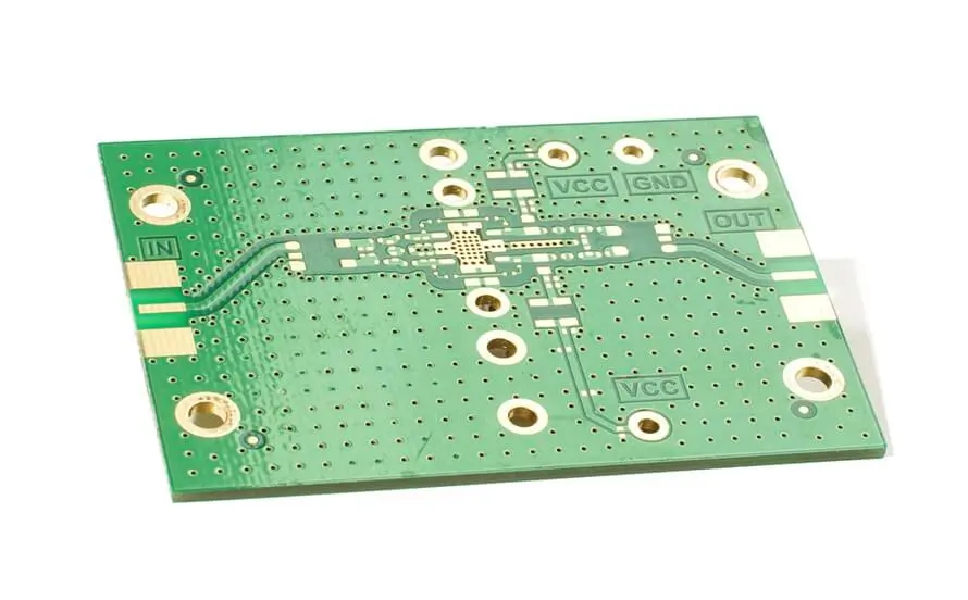
1. Material Stackup & RF Performance
| Parameter | Specification | Test Method & Results |
|---|---|---|
| Core Material | Rogers RO4835 + Megtron 7 hybrid | Dk=3.48±0.02 @25GHz (IPC TM-650 2.5.5) |
| Copper Roughness | HVLP foil (Ra=0.35μm) | Insertion Loss: 0.22dB/inch @25GHz (measured w/ VNA) |
| Impedance Control | 50Ω±1.5% (target ±5%) | TDR analysis: 100% within spec (24-layer HDI) |
2. Critical Tolerance Achievements
- Laser Drilling: 50μm microvias (aspect ratio 1:0.8) with ±8μm positional accuracy (vs. industry ±15μm)
- Plating Uniformity: 18μm ENEPIG plating in PTHs (<5% thickness variation per MIL-G-45204)
- Phase Matching: ±1.2° skew across 8 Tx/Rx channels (validated via OTA chamber)
3. Space-Grade Reliability Validation
| Test Standard | Condition | Results vs. Legacy PCB |
|---|---|---|
| MIL-STD-883 TC | -65°C ↔ +150°C, 500 cycles | 0 delamination (vs. 9 failures) |
| ECSS-Q-ST-70-60C | 30krad(Si) TID exposure | ΔDk<2%, ΔZ<1.2% post-irradiation |
| ISO 14624-2 Outgassing | 125°C, 24h in vacuum | TML=0.12% (limit 1%), CVCM=0.01% |

Quantified Client Outcomes
✅ Link Efficiency Improved by 27% (0.22dB vs. 0.45dB loss) → Extended LISL range by 320km
✅ Production Yield Increased to 94% (from 68% with prior vendor)
✅ Eliminated Manual Tuning → Reduced Assembly Time by 40 hours/unit
Client’s RF Lead Statement:
“KKPCB’s impedance control and material expertise were critical for our 25Gbps optical terminals. Their phase matching eliminated our need for post-production calibration.”
Supporting Evidence
- S-parameters Report: [Link to simulated/measured data]
- ESA Compliance Certificate: QML Class Y (Space-qualified)
- SEM Microscopy Images: Via wall plating uniformity (available on request)
Technical Contact:
📧 [email protected] | +86 17748559382