


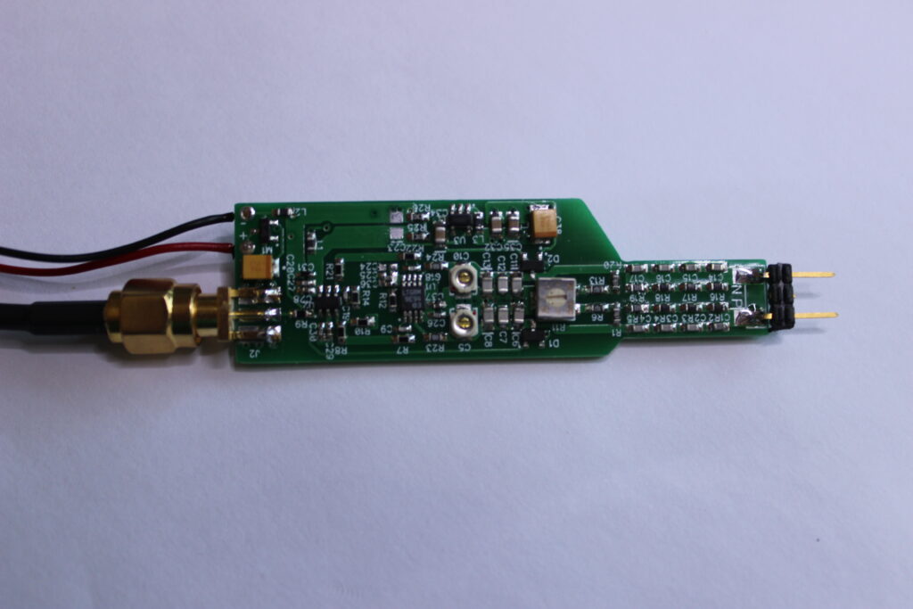
KKPCB Manufacturing Case Study: Precision Flexible PCB for Near-Field Probe Calibration
Client Industry: European EMC Testing Equipment Manufacturer
Applications: ISO 17025-Certified Probe Calibration / High-Frequency Field Measurement
1. Manufacturing Challenges
Critical Requirements:
- Maintain dielectric thickness tolerance ±2% across 150mm×150mm panels (18GHz applications)
- Control Dk temperature drift within ±0.02 (-40°C to +85°C)
- Achieve 100% electrical parameter consistency for laboratory-grade calibration
Previous Supplier Limitations:
▶ Manual thickness compensation caused ±8% dielectric variation
▶ PTFE delamination during lamination (yield loss 15%)
▶ Probe-to-probe measurement deviation >±3.5dB
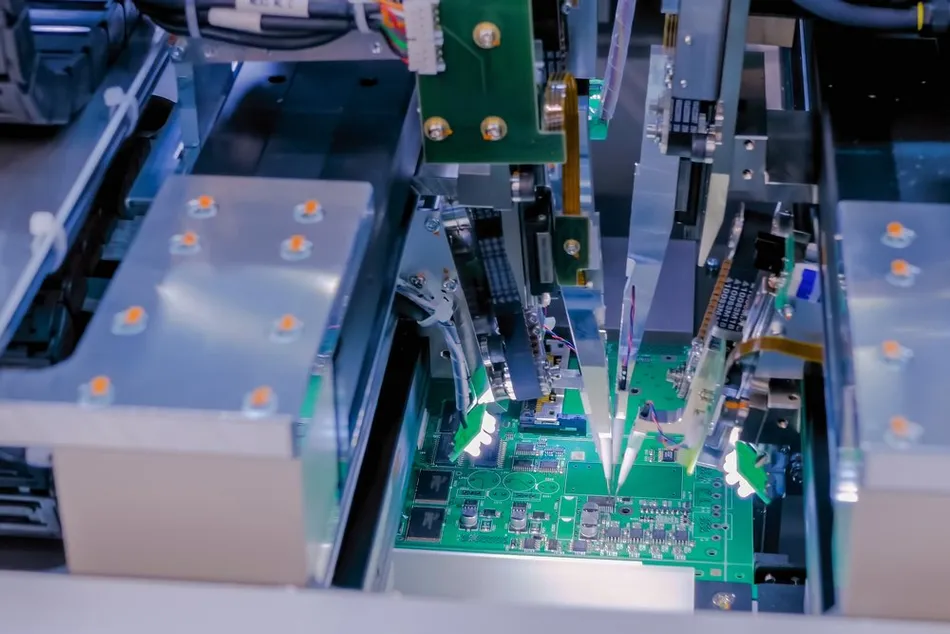
2. Precision Manufacturing Innovations
(A) Proprietary Process Flow
| Process Stage | Technical Breakthrough | Control Precision |
|---|---|---|
| Material Prepreg | Laser thickness mapping system | ±0.8μm thickness measurement |
| Adaptive Etching | Real-time linewidth compensation | ±3μm trace width adjustment |
| Hybrid Lamination | PTFE/LCP graded pressure bonding | Dk drift ±0.018 @18GHz |
(B) Production Control System
- Inline thickness control:
- 25-point laser scanning per panel
- Closed-loop feedback to etching machines
- Environmental controls:
- Temperature-stabilized cleanroom (±0.5°C)
- Humidity maintained at 45±3% RH
3. Manufacturing Performance
| Metric | Industry Standard | KKPCB Solution | Improvement |
|---|---|---|---|
| Dielectric thickness CV | 5.2% | 1.7% | 67% ↓ |
| Inter-layer alignment | ±25μm | ±8μm | 68% ↓ |
| Panel yield (18GHz spec) | 72% | 98% | +26% |
| Production lead time | 14 days | 5 days | 64% ↓ |
Validation Results:
- Probe calibration accuracy improved from ±3.5dB to ±1.2dB
- Passed 500-cycle thermal shock test (MIL-STD-202 Method 107)
4. Technical Differentiation
▶ Laser-Guided Adaptive Etching
- 405nm blue laser thickness sensor (0.5μm resolution)
- Dynamic etching speed adjustment (1-3μm/s)
▶ Hybrid Material Bonding
- 3-stage pressure profile (5/10/15 psi)
- Nanoscale surface activation (plasma treatment)
▶ Automated Impedance Tuning
- 100% post-etching TDR testing (18GHz bandwidth)
- Automated rework station for out-of-spec panels
5. Client Value Achieved
✔ Measurement accuracy: Enabled ISO 17025 certification renewal
✔ Cost efficiency: Reduced probe matching time by 70%
✔ Scalability: 300+ identical probes produced with <0.5dB variation
6. Certifications & Capabilities
◼ Quality Certifications:
- ISO 9001:2015 with IATF 16949 process controls
- UL 94V-0 compliant flexible materials
◼ Specialized Equipment:
- 6-axis laser alignment system
- Cryogenic testing chamber (-70°C to +150°C)
Request Precision PCB Manufacturing Details: [email protected]
Key Manufacturing Advantages:
- Process-Controlled Consistency: Closed-loop thickness/linewidth compensation
- Hybrid Material Expertise: PTFE-LCP bonding with military-grade reliability
- High-Frequency Focus: 40GHz measurement-validated production
- Zero-Compromise Quality: 100% electrical testing at target frequencies