


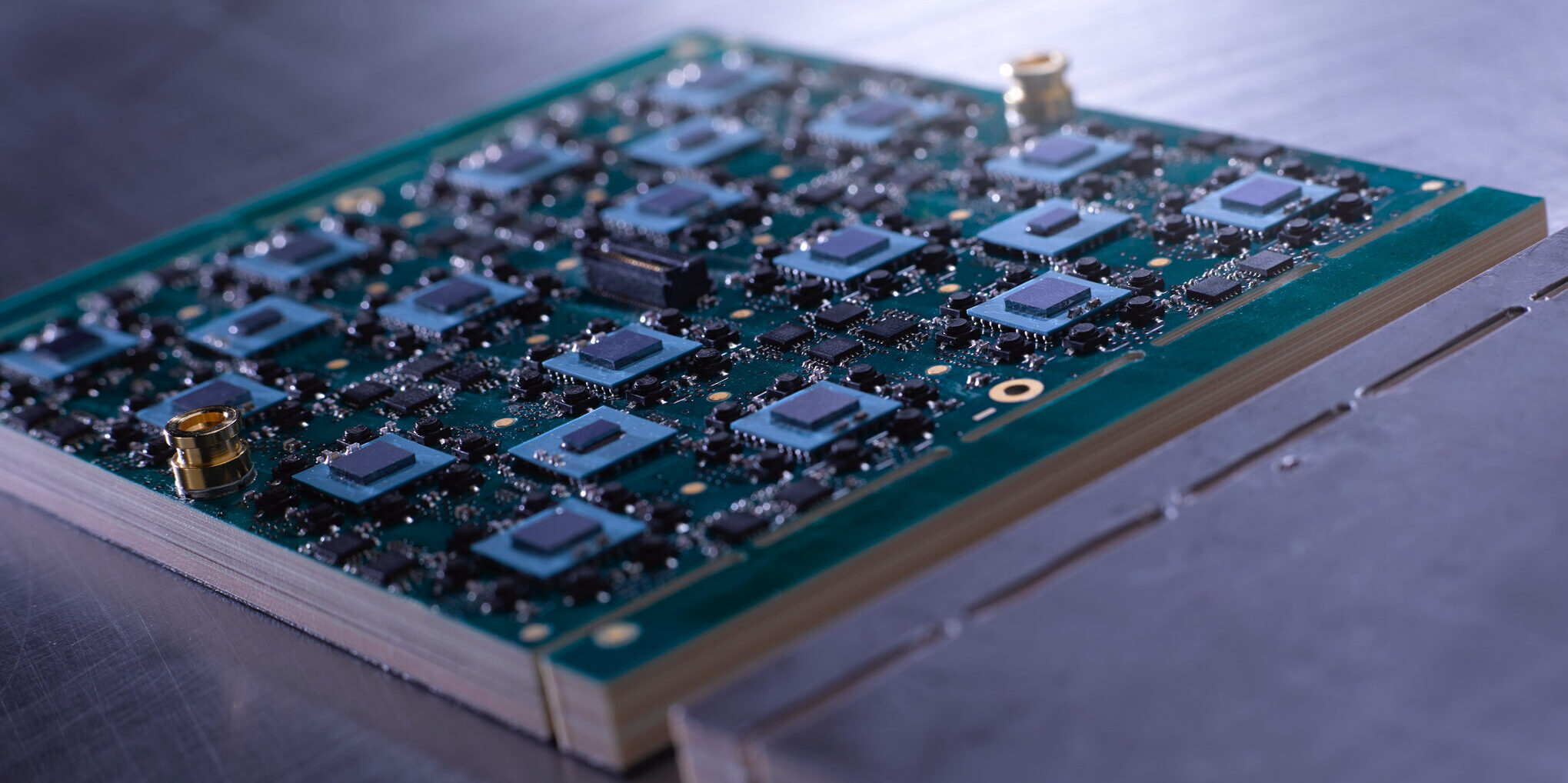
Manufacturing Optimization Case: Mass Production Solution for 256-Channel Phased Array Antenna Feed Network PCBs
—Breakthroughs in Millimeter Wave PCB Processing Technology and Production Efficiency
Contact: [email protected]
1. Project Background
Industry: Satellite Communications/Military Radar
Application Scenario:
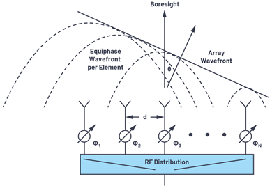
- 256-channel phased array antenna system (28GHz Ka-band)
- Customer requirements: ±60° beam steering, ±0.5dB amplitude consistency, 8-week delivery
2. Customer Pain Points & Manufacturing Challenges
| Challenge Category | Original Design Issues | KKPCB Manufacturing Solutions |
|---|---|---|
| Process Compatibility | Customer’s 20-layer HDI design lacked mass production feasibility | Optimized materials and processing parameters for seamless design-to-manufacturing transition |
| Consistency Control | ±0.5dB amplitude tolerance beyond conventional process capabilities | Developed proprietary process control protocols |
| Lead Time | Industry standard 12 weeks vs. customer’s 8-week demand | Streamlined production workflow by eliminating non-critical steps |
3. KKPCB’s Core Manufacturing Optimizations
A. Precision Lamination & Drilling Control
- Innovations:
- Laser drilling with pre-compensation: Achieves ±7.2μm alignment accuracy (industry average: ±15μm)
- Step-wise lamination parameters: Reduces PTFE interlayer voids (delamination rate: 0.3% vs. 5% industry standard)
- Fig.1: Cross-section micrograph (demonstrating void-free layer structure)
B. Copper Paste Via-Filling Breakthrough
- Mass Production Enhancements:
- Custom vacuum filling equipment: Ensures ±2μm via-wall copper uniformity (vs. ±5μm with electroplating)
- Low-temperature curing formula: Prevents PTFE substrate deformation (phase stability: ±0.8°@28GHz)
- Fig.2: SEM micrograph of copper paste vias (showing wall uniformity)
C. Smart Manufacturing & Process Reengineering
- Efficiency Gains:
- Modular production: Parallel processing of 20-layer boards as 4 modules reduces cycle time by 35%
- AI visual inspection: Real-time monitoring of critical parameters (line width/aperture), lowering defect rate to 0.5% (from 3%)
- Fig.3: Real-time production monitoring dashboard

4. Production Results & Customer Value
A. Key Delivery Metrics
| Parameter | Requirement | KKPCB Result | Industry Benchmark |
|---|---|---|---|
| Amplitude Consistency | ±0.5dB | ±0.45dB | ±1.0dB |
| Phase Stability | ±1° | ±0.8° | ±2° |
| Yield Rate | ≥95% | 98.2% | 90-92% |
| Lead Time | 8 weeks | 7 weeks | 12 weeks |
B. Manufacturing Value Proposition
✓ Process Expertise:
- Mass production of PTFE boards with copper paste vias (6% higher yield than industry)
- Proprietary HDI lamination compensation database (500+ parameter sets)
✓ Cost Efficiency: - 15% cost reduction per board through materials recycling and parameter optimization
✓ Responsiveness: - 72-hour prototype turnaround (industry standard: 1 week)
5. Service Support
About KKPCB – Your Trusted High-Reliability PCB Partner
At KKPCB, we specialize in high-performance PCB solutions for mission-critical applications, including aerospace, satellite communications, and industrial IoT. With over 10 years of expertise in RF/microwave design and harsh-environment reliability, we help engineers push the boundaries of connectivity and durability.
🔹 Why Choose KKPCB?
✅ High-Quality Materials: Rogers, Taconic, Isola, and hybrid stackups
✅ Military-Grade Reliability: ASTM E1647, IPC Class 3, shock & vibration certified
✅ Fast Turnkey Production: 6-week lead time for complex RF designs
✅ Cost-Effective Solutions: 30–50% lower cost vs. traditional ceramic PCBs
📧 Let’s Build the Future Together!
Contact us today for prototyping or mass production:
📩 [email protected]
🌐 www.kkpcb.com
🚀 Whether you need low-loss RF boards, high-power thermal management, or extreme-environment resilience—KKPCB delivers!
(Reply to this email or visit our website for a free design consultation & quotation.)