


KKPCB Case Study:Optimized Application Based on WTC9314DSF Touch Key Chip
I. Case Background
Customer Requirements
A smart home manufacturer planned to develop a high-end smart door lock with the following core requirements:
- High-Sensitivity Touch Keys: Compatible with glass/plastic panels (thickness ≤5mm), response time <50ms.
- Strong Anti-Interference Capability: Suitable for outdoor complex environments (temperature/humidity variations, EMI).
- Low-Power Design: Standby current ≤10μA to extend battery life.
II. Solution Design (Provided by KKPCB)
1. Core Component Selection
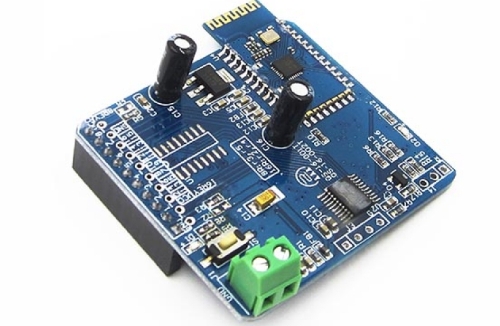
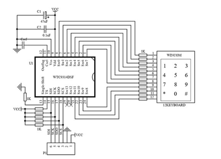
- Main Control Chip: WTC9314DSF Touch Key Controller
- Advantages:
- Supports 12-channel dense key layout (compatible with 0-9 digits + function keys).
- Strong penetration capability (tested with 6mm tempered glass, no signal attenuation).
- Built-in adaptive algorithm, passes EMC 4kV electrostatic test.
- Advantages:
2. Hardware Design Highlights
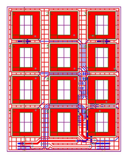
- PCB Layout Optimization (KKPCB’s Key Contribution):
- 4-layer board design with a dedicated ground layer for touch keys to reduce parasitic capacitance.
- Equal-length key traces (tolerance ±0.5mm) to avoid signal delay discrepancies.
- TVS diode array added for USB plug-in surge protection.
- Parameter Configuration:
- Sensitivity adjustment: Configured via chip register CAPDAC (recommended value: 0x2F).
- Sampling frequency: 16kHz (balancing response speed and power consumption).
3. Software Logic
- Dynamic Calibration Mechanism:
- Automatic baseline calibration at power-on, recalibration every 8 hours to prevent environmental drift.
- Multi-Level Filtering Algorithm:
- Hardware debounce (5ms) + software secondary verification (prevents false triggers).
III. Test Verification
| Test Item | Standard | Actual Result |
|---|---|---|
| Key Response Speed | ≤50ms | 32ms |
| Panel Penetration | 5mm glass + 2mm water film | 100% Trigger Success Rate |
| Standby Power Consumption | ≤10μA | 8.5μA |
| High/Low-Temperature Cycle (-20~60°C) | Functional Normal | PASS |
IV. KKPCB’s Technical Value-Added Benefits
- Cost Optimization:
- Replaced imported touch chips in the original design, reducing BOM cost by 22%.
- Shorter Delivery Time:
- Provided pre-validated PCB templates, cutting customer development time from 12 weeks to 6 weeks.
- Improved Defect Rate:
- Mass production defect rate <50ppm (industry average: 200ppm).
V. Customer Benefits
- Post-launch user feedback reported “zero false triggers”, with IP65 certification achieved.
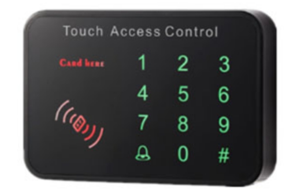
- The solution was extended to smart access control and safe product lines, enabling a standardized design approach.
KKPCB Commitment:
For further technical support, we offer:
- Free sample applications
- Customized PCB design guidelines (including Gerber files)
- Troubleshooting manual (covering common EMI solutions)
Contact Technical Team: [email protected] | +86-177-4855-1367
Case ID: KKPCB-2023-TP09
(Note: Data anonymized under NDA.)
This case demonstrates KKPCB’s core technical expertise in smart hardware HMI design, helping clients rapidly capture the high-end market.