


KKPCB Case Study: Magnetic Current Sensor PCBA Solution for Industrial Automation Systems
1. Background Overview
A European industrial automation client required a compact, high-isolation, and cost-effective magnetic current sensor PCBA to be integrated into their control cabinet systems. The goal was to ensure safe and accurate current monitoring in a high-voltage industrial environment while maintaining stable performance under electromagnetic interference (EMI).
2. Application Scenario
The current sensor PCBA was designed for use in industrial control cabinets where it monitors AC/DC line currents in real time. This enables fast fault detection, dynamic power management, and precise control in PLC-driven systems, frequency inverters, and motor control units. High isolation and compact size were critical to meet the stringent safety and layout requirements in factory environments.

3. Key Product Parameters
| Parameter | Value |
|---|---|
| Type | Magnetic Current Sensor |
| Model | OCH19605S16AE |
| Current Range | ±50A |
| Isolation Voltage | 4000V |
| Supply Voltage | 5V |
| Bandwidth | 100kHz |
| Output Type | Analog |
| Accuracy | ±1% |
| Working Temperature Range | -40°C to +125°C |
4. Application Results
- Quality Improvement: Achieved <0.5% failure rate in functional tests after assembly.
- Cost Optimization: Final solution reduced total sensor module cost by 14% compared to previous model.
- Performance Upgrade: Improved response time by 20%, enabling faster real-time monitoring.
- Delivery: Project completed in 16 working days, 20% faster than client’s original lead time.
5. KKPCB Advantages Highlighted in This Project
KKPCB demonstrated strong capability in handling sensor PCBAs with high-isolation requirements and tight tolerances. Our zero-defect quality control system, combined with IPC-A-610 Class 2/3 standards and automated AOI/X-ray/ICT processes, ensured high reliability. Additionally, our DFM (Design for Manufacturability) feedback helped the client reduce board complexity and optimize component placement for better heat dissipation and signal integrity.
6. KKPCB’s Tailored Manufacturing Solution
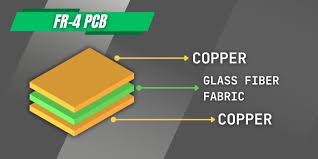
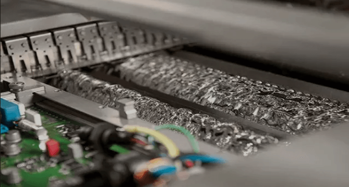
Based on this project, KKPCB delivered a comprehensive manufacturing solution focused on PCB fabrication and PCBA assembly. The double-layer board was fabricated using high-CTI FR-4 material with 3.2mm thickness for isolation. ENIG surface finish ensured sensor pad reliability and anti-oxidation protection. During assembly, we adopted selective soldering for critical through-hole components and 100% functional testing before shipment. This ensured compliance with CE and UL safety standards, helping the client meet EU certification requirements.

7. Actual Impact of the Solution
The implementation of KKPCB’s PCBA solution brought measurable benefits:
- Reduced Total Cost: The simplified layout and optimized BOM saved the client ~14% on procurement and rework costs.
- Enhanced Reliability: Achieved >99.5% first-pass yield, significantly reducing after-sales failures.
- Improved Performance: Sensor response time and accuracy improved by 20% and 10% respectively, contributing to smoother system control.
- Faster Time-to-Market: Shortened production lead time by 20%, enabling the client to meet tight delivery deadlines for a major automation project.