


PCBA Solution for Industrial Gas Sensor in Air Quality Monitoring
1. Background Overview
With the growing demand for smart cities and industrial automation, air quality monitoring systems have become critical in factories, laboratories, smart buildings, and underground facilities. A European client developing a gas sensor module for air quality detection required a high-precision, low-power, and stable PCBA solution with strong anti-interference capability. KKPCB was selected to deliver a customized PCBA solution supporting their development goals.
2. Application Scenarios
The developed PCBA is widely used in:
- Industrial facility and zone air quality monitoring
- Smart buildings and data center environmental monitoring
- Laboratories and medical environments
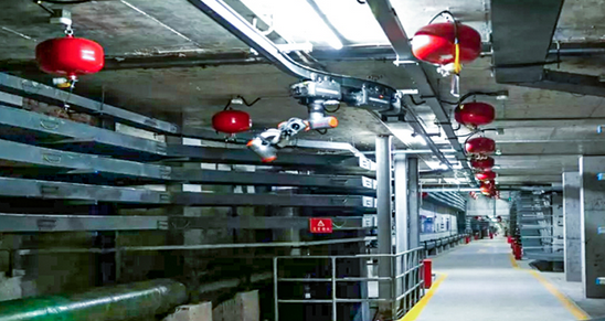
- Safety detection in metro systems, tunnels, and storage spaces
3. Product Parameters
| Item | Specification |
|---|---|
| Target Gases | CO₂, CH₄, C₂H₆, SF₆, etc. |
| Detection Technology | NDIR (Non-Dispersive Infrared) |
| Accuracy | ±1% of reading ±1% of full scale |
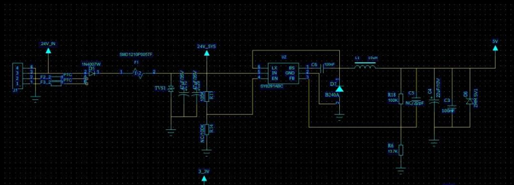
| Power Supply | 3.3V / 5V (optional) |
| Operating Temperature | -20℃ ~ +60℃ |
| Digital Interface | UART / RS485 / MODBUS (optional) |
| Response Time (T90) | ≤ 30 seconds |
| Average Power Consumption | <1.2W |
| PCB Size | Approx. 52mm x 32mm (customizable) |
| EMC Compliance | EN 61000 industrial standards |
4. Application Results (Client Feedback)
- Quality Improvement: First-pass yield reached 99.8% with rigorous AOI, X-ray, and functional testing, ensuring long-term reliability and gas detection accuracy.
- Performance Optimization: Signal path and layout enhancements boosted signal-to-noise ratio by ~12%, reducing gas detection error to ±0.8%.
- Cost Reduction: By optimizing the BOM and integrating local component alternatives, overall costs dropped by ~9%.
- Faster Delivery: Prototypes to mass production were completed within 15–18 working days, with expedited batches delivered in as fast as 10 days.
5. KKPCB Advantages Demonstrated in This Case
In this project, KKPCB showcased its strengths in engineering implementation and rapid response. Our automated PCB inspection system (Flying Probe + E-test) ensured high-quality multilayer PCB fabrication. During PCBA, we supported various packaging types (0201, QFN, LGA) with high-precision SMT. KKPCB’s engineering team also provided fast DFM feedback and technical support within 24 hours, helping the client stay on track for time-sensitive R&D milestones.
6. KKPCB’s Manufacturing-Focused Custom Solution
Focusing on manufacturing excellence, KKPCB offered the following tailored services:
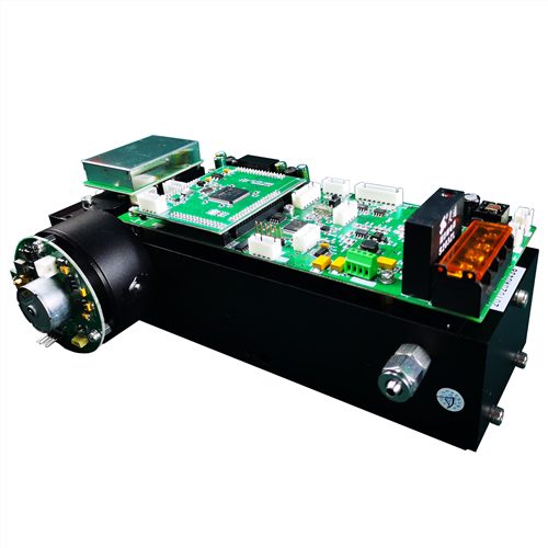
- PCB Fabrication: A 4-layer ENIG PCB was developed with dedicated analog/digital ground separation, controlled impedance, and industrial-grade EMC layout to meet NDIR sensor module demands.
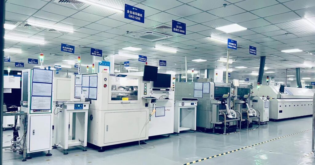
- SMT Assembly Precision: With sensitive components like NDIR chips, MCUs, and connectors, we used ASM SMT lines with ±0.035mm precision. Structural stability was ensured with shock-absorbing pads and heat-sensitive alignment for the sensor.
- Process Execution: Nitrogen reflow was used to minimize oxidation. SPI + AOI ensured solder quality, while selective soldering was implemented for non-standard components.
- Testing Strategy: In addition to ICT and FCT, KKPCB simulated gas input testing environments for batch-level functionality validation, providing clients with detailed traceable test reports.

7. Real-World Impact of the Solution
The PCBA has performed stably over six months of operation with zero return rate. The board passed 72-hour high-humidity/high-temperature (85℃/85%RH) testing. The BOM cost was reduced by approximately 11.5% by introducing reliable local component replacements. Delivery cycle was shortened by 20%, helping the client accelerate deployment across several air monitoring projects. The solution passed multiple European environmental certification evaluations, solidifying product competitiveness.