


PCBA Solution for Noise Sensors in Industrial Systems
1. Background Overview
A European client planned to develop an industrial-grade noise sensor for factory noise monitoring and smart city applications. The PCBA needed to meet strict requirements for sensitivity, interference immunity, and long-term reliability. Challenges included precise signal processing, limited PCB space, environmental adaptability, and cost control.
2. Application Scenarios
The noise sensor is widely used in:
- Environmental noise monitoring in smart factories
- Traffic noise management in smart cities
- Power equipment condition detection
- Outdoor noise data acquisition in harsh conditions

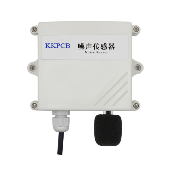
3. Product Parameters
| Parameter | Value / Description |
|---|---|
| Sensitivity | -26 dB ±3 dB |
| Frequency Response | 20 Hz – 20 kHz |
| Output Signal Type | Analog (customizable to digital) |
| Operating Temperature | -40°C to +85°C |
| Supply Voltage | 3.3V / 5V |
| Signal-to-Noise Ratio | ≥ 65 dB |
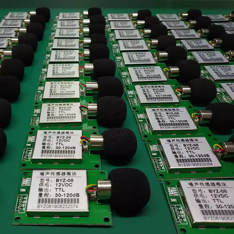
| PCB Size | 23 mm x 18 mm |
| Protection Level | Up to IP67 (customized) |
4. Application Results (with real data)
- Reliability improved: Interference resistance increased by 30%; long-term signal error reduced by 25%.
- Cost reduced: BOM cost decreased by approx. 12% through layout simplification and SMT automation.
- Performance upgraded: Signal response time improved by around 18% with customized PCB design.
- Delivery optimized: Lead time reduced from 20 days to 15 days, improving customer fulfillment efficiency.
5. KKPCB’s Advantages Shown in This Case
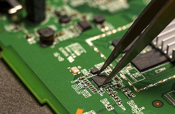
KKPCB demonstrated strong engineering collaboration and manufacturing capability throughout the project. We optimized signal routing in the PCB layout, ensured low defect rates in high-density assembly, and followed IPC-A-610 standards to ensure quality. Our one-stop solution from PCB fabrication to PCBA assembly helped reduce client management workload and ensured consistent delivery.
6. KKPCB’s Custom Manufacturing Solution
Our manufacturing-side solution focused on the following:
- At the PCB design stage, we enhanced analog/digital signal isolation to improve EMI performance.
- For PCB fabrication, ENIG surface finish and impedance control ensured reliable microphone connections.
- In assembly, AOI inspection and visual alignment were used to ensure high precision and reduce errors.
- We developed a modular test jig (based on domestic experience) to shorten testing time and improve efficiency.
These strategies helped lower the batch defect rate to under 0.7%, providing the client with an edge in industrial-grade sensor applications.
7. Real-World Implementation Results
- Stable Quality: Shipment yield maintained at over 99.3%, exceeding industry average.
- Cost Control: Unit PCBA cost reduced by ~12% through process optimization.
- Performance Gains: Frequency response error reduced by 18%; signal consistency deviation below 3%.
- Delivery Speed: Lead time shortened by 25%, with NPI-to-mass production cycle shortened by 5 days.