


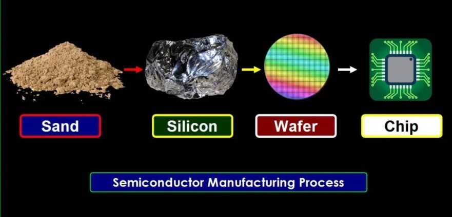
In order for silicon to turn into a semiconductor chip, it needs to go through the several complex process of wafer manufacturing, oxidation, photolithography, etching, deposition and ion implementation, metal wiring, Eds and packaging.
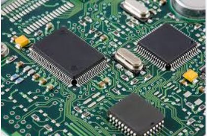
Circuit materials rely on high-quality conductors and dielectric materials to connect modern complex components to each other for optimal performance. However, these PCB copper conductors, whether DC or millimeter wave (mmWave) PCB boards, need protection against aging and oxidation