


In the world of PCB manufacturing, two main methods are commonly used: PCB prototyping and standard PCB production. Both methods play critical roles and come with their own characteristics. Reducing the time and costs associated with the development process can significantly increase the success rate of future projects. This article explores the benefits of starting with a prototype PCB for design verification before transitioning to standard PCB production assembly.
Designing a high-voltage PCB requires careful planning, adherence to specific guidelines, and a keen eye for safety. Whether you’re working on industrial equipment, power electronics, or consumer devices, the following tips and considerations will ensure you create efficient and safe high-voltage PCB designs.

Solar energy is rapidly gaining popularity as an alternative energy source. One of the key components of a solar energy system is the solar inverter. A solar inverter is a device that converts the direct current generated by solar panels into alternating current
In conclusion, managing EMI and ensuring EMC are critical aspects of PCB design and manufacturing. By carefully considering factors like trace routing, grounding, component selection, and shielding, designers can minimize the risks associated with electromagnetic interference and create devices that perform reliably and safely.
Motor driver ICs handle high currents and dissipate substantial heat, so efficient PCB design is essential to ensure proper heat dissipation and reliable performance. Below are some best practices for designing a robust PCB for motor driver ICs.
The output value of the global electroplating PCB industry accounts for the rapid growth of the proportion of the total output value of the electronic component industry. It is the industry with the largest proportion in the electronic component industry. It occupies a unique position
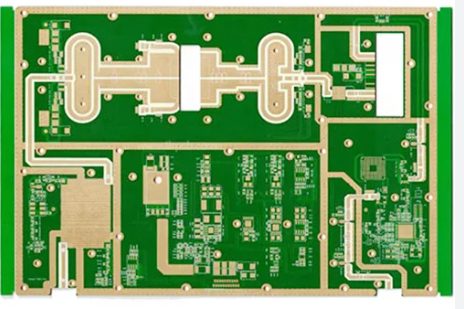
Multilayer PCBs (Printed Circuit Boards) are integral to modern electronics, offering unparalleled performance in compact designs. While they come with several benefits, they also present unique challenges.
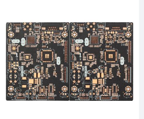
Multilayer Printed Circuit Boards (PCBs) or Multilayer Boards (MLBs) feature more than two copper layers, interconnected using copper-plated holes. These holes may include NC vias, laser microvias, through-holes, buried, or blind vias. The layers consist of copper foil, prepreg (PP), or adhesive materials and are pressed together under high temperature and pressure. This process removes air and cures the thermosetting adhesives, forming a cohesive multilayer PCB
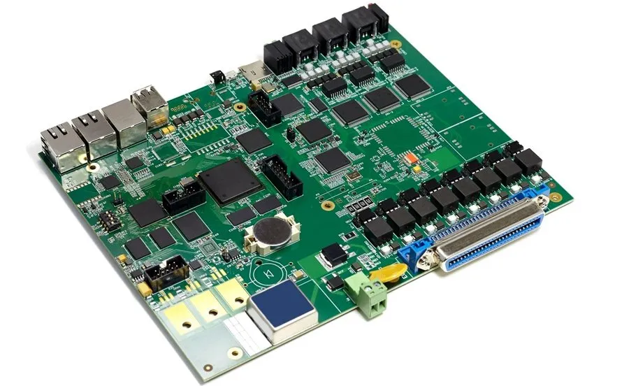
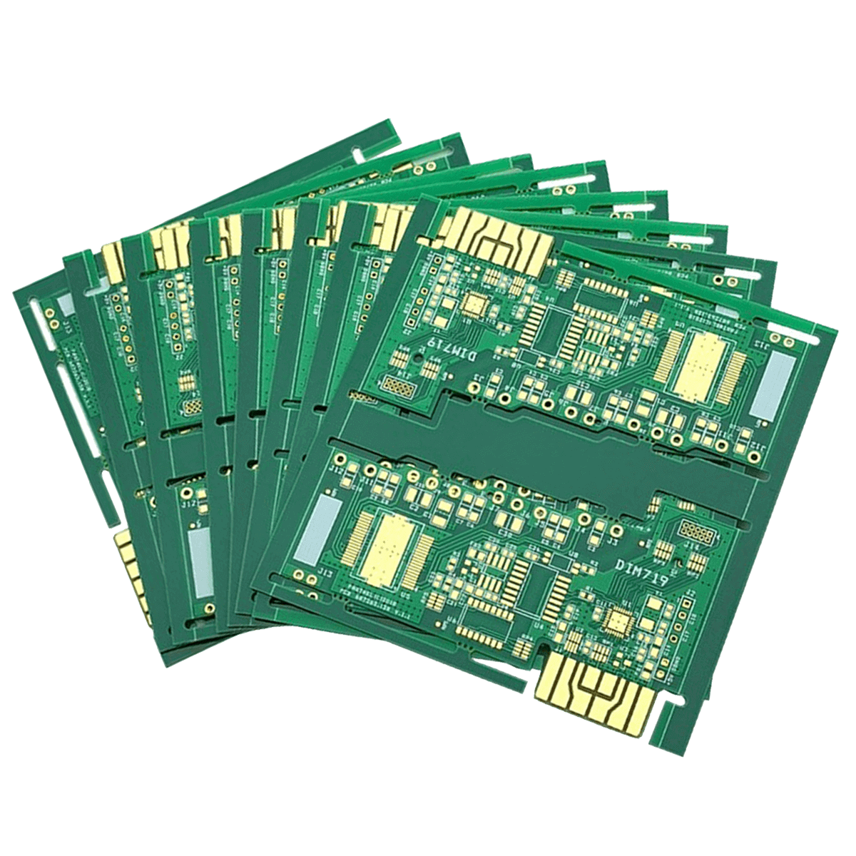
KKPCB provides global customers with one-stop services from PCB layout, prototype PCB proofing, PCB manufacturing, PCBA processing (including SMT and DIP), PCBA testing, PCBA product assembly and outbound packaging. You could provide a Gerber file or BOM list to us, we will offer the finished PCB products or PCB assembly which are satisfied with you
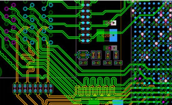
PCB design requires understanding physical processes and careful organization of layers, power networks, and signal paths. Following these recommendations reduces noise risk, improves reliability, and simplifies the routing of complex systems