


Careful adherence to these guidelines ensures efficient and reliable mobile phone PCB designs. By prioritizing critical signal paths, ensuring proper grounding, and optimizing power distribution, potential risks in wiring are mitigated, resulting in better performance and reduced EMI issues.
Electromagnetic interference (EMI) control is critical in high-speed PCB design, and one often-overlooked aspect is the influence of integrated circuit (IC) packaging. Incorporating decoupling capacitors within the IC package can effectively reduce EMI and enhance signal integrity. This guide delves into the role of IC packaging in EMI suppression, exploring the root causes of EMI, key IC package design considerations, and practical design rules to optimize performance.
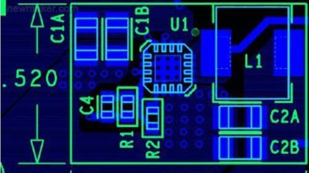
In power supply design, PCB layout plays a critical role in ensuring the circuit’s efficiency, stability, and reliability. Below are five essential considerations for effective PCB design in power supply applications:
Effective PCB design for single-chip microcontroller (MCU) control boards involves structured layout and routing principles to minimize interference and enhance performance. Proper planning of input/output paths, decoupling, grounding, and component placement is crucial.
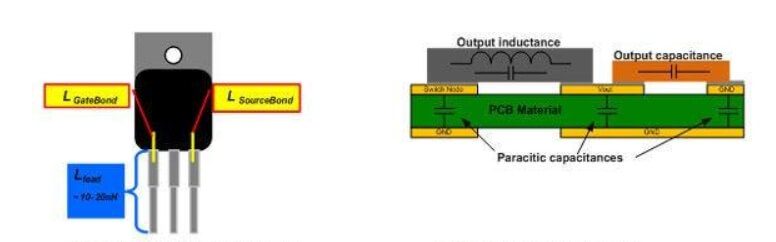
Based on recent trends, improving efficiency is a key goal, and the trade-off of using slow switching devices for better EMI is not worth it. Superjunctions can improve efficiency in applications where planar MOSFETs struggle. Superjunction MOSFETs significantly reduce on-resistance and parasitic capacitance compared to traditional planar MOSFET technology. The significant reduction in on-resistance and reduced parasitic capacitance, while helping to improve efficiency, also produces fast switching transitions of voltage (dv/dt) and current (di/dt), forming high-frequency noise and radiated EMI.
As electronic products become more advanced, they encounter more sources of electromagnetic interference (EMI) that can disrupt device function and potentially harm health. This guide explores strategies for designing PCB boards with optimized electromagnetic compatibility (EMC), focusing on reducing interference and increasing product resilience.
Before explaining the inspection work after PCB wiring is completed, we will first introduce three special PCB routing techniques. The routing of PCB LAYOUT will be explained from three aspects: right-angle routing, differential routing, and serpentine routing
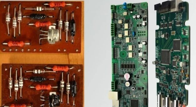
PCB design translates electrical schematics into a functional product, and its quality directly impacts production efficiency and product reliability. For beginners, mastering PCB layout can be challenging despite familiarity with design software, and common issues often arise. Here, seasoned engineers from KKPCB share their PCB layout insights to help avoid these pitfalls and inspire best practices.
By following these guidelines—such as optimizing trace width, minimizing via use, and ensuring proper documentation for manufacturing—you can significantly improve the performance, reliability, and manufacturability of your PCB designs.
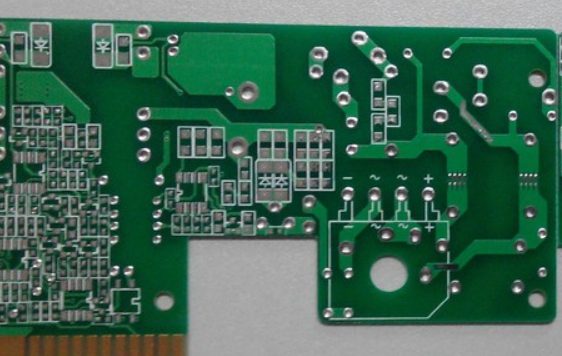
PCB design involves two critical stages: component layout and circuit connection wiring. The layout is the arrangement of circuit components within the PCB’s wiring area. A well-thought-out layout directly affects the ease of subsequent wiring and significantly impacts the PCB’s overall performance. In addition to meeting circuit functionality and performance requirements, a good layout considers manufacturability, inspection, and maintenance. Components should be placed evenly, neatly, and compactly, ensuring that leads and connections are short, minimizing interference and signal transmission delays.