


Thermostats are an essential part of our daily lives and industrial systems, regulating temperature to maintain stable conditions in both equipment and environments. However, to ensure thermostats operate reliably under various conditions, the core technology behind them—PCB (Printed Circuit Board) design—must meet high standards. This article explores the key factors to consider when designing a thermostat PCB and how to ensure its efficient and reliable performance.
RF and microwave PCB assemblies are widely recognized as the go-to solutions for networking and communication due to their superior ability to handle high frequencies. Their capacity to operate in the megahertz (MHz) to gigahertz (GHz) range makes them indispensable for modern communication applications.
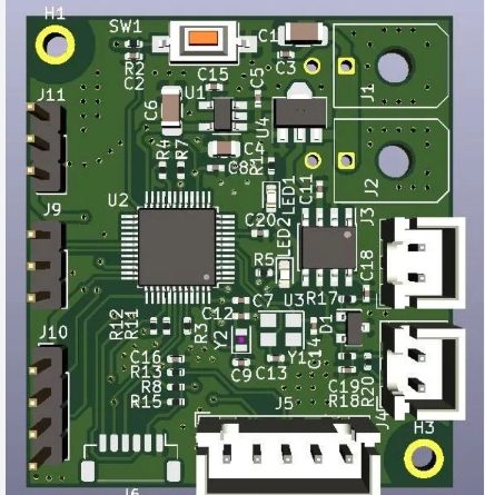
In the era of smart manufacturing, industrial robots are transforming the production landscape with enhanced efficiency, precision, and safety. Central to this evolution is the indispensable role of printed circuit boards (PCBs). Acting as the “nervous system” of robots, PCBs support signal transmission, control functions, and intelligent decision-making. As robotics technology advances, so too does the design and functionality of PCBs.
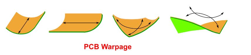
Printed Circuit Board (PCB) warpage refers to the phenomenon that the PCB plane bends or deforms due to various reasons during the manufacturing, storage or use of the PCB. This deformation may be local or overall, and is usually manifested as the PCB no longer remaining flat.
As electronic devices become more complex and ubiquitous, the need for reliable and high-performance PCBs continues to grow. PCB testing standards provide a framework for ensuring that these essential components meet industry benchmarks for safety, reliability, and functionality. Manufacturers who adhere to these testing standards are better positioned to deliver high-quality, dependable products, build trust with their customers, and minimize the risk of product failures. Whether through visual inspection, electrical testing, or advanced X-ray analysis, rigorous testing ensures that the PCBs will perform as expected, even in the most challenging environments.
As the largest PCB manufacturer globally, China not only leads in production volume and technology but also continues to innovate. By increasing research and development investment and optimizing production processes, China’s PCB industry has gradually transitioned from low-end manufacturing to high-end production, especially excelling in areas such as high-frequency, high-speed, and high-precision applications. Meanwhile, China’s cost advantages, rich industrial chain resources, and mature supply chain management systems further solidify its dominant position in the global market.
The Internet of Things (IoT) is revolutionizing industries worldwide, and its influence on Printed Circuit Board (PCB) design and manufacturing is profound. As IoT devices become more compact, efficient, and interconnected, the demand for innovative PCB designs has surged. This blog delves into how IoT is transforming PCB design and manufacturing, the challenges it poses, and the opportunities it presents.
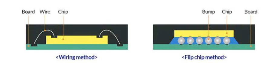
The base material of IC packages is the integrated circuit substrate (or IC package substrate). They shield the bare IC while supporting interconnection between the IC and the PCB’s trace network. As a result, the substrate has a significant impact on circuit performance
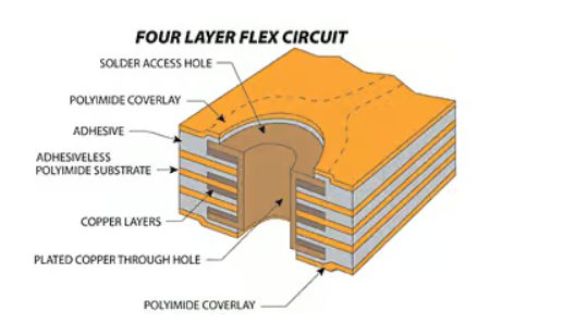
Flexible printed circuits (FPCs) provide invaluable dynamic flexing and shape conforming capabilities in electronics. 4 layer flex PCBs with conductors on 4 layers enable increased routing density and integration versus 2 layer flex, while retaining excellent flexibility.
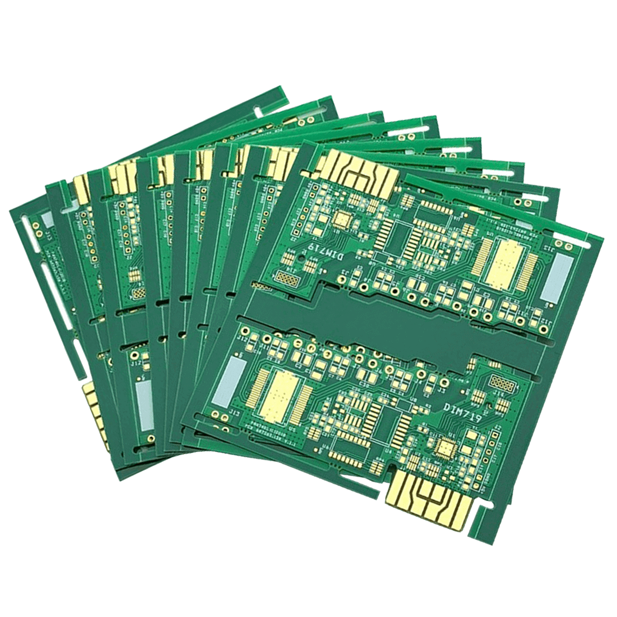
Multilayer Printed Circuit Boards (PCBs) or Multilayer Boards (MLBs) feature more than two copper layers, interconnected using copper-plated holes. These holes may include NC vias, laser microvias, through-holes, buried, or blind vias. The layers consist of copper foil, prepreg (PP), or adhesive materials and are pressed together under high temperature and pressure. This process removes air and cures the thermosetting adhesives, forming a cohesive multilayer PCB