


Industry: Defense Electronics
End Applications:
Armored vehicle main control units
Field communication relay equipment
Manufacturing Challenges:
Heterogeneous material processing (AlSiC metal substrate + FR4 multilayer hybrid lamination)
Extreme environment reliability (MIL-STD-810H vibration compliance)
Military-grade quality control (100% inspection + batch traceability)
Previous Supplier Pain Points:
✔ AlSiC substrate yield only 65% (delamination due to CTE mismatch)
✔ PCIe gold finger contact failure rate 3,000 PPM (post-vibration)
✔ EMP shielding layer vacuum lamination yield below 80%
1. Project Background
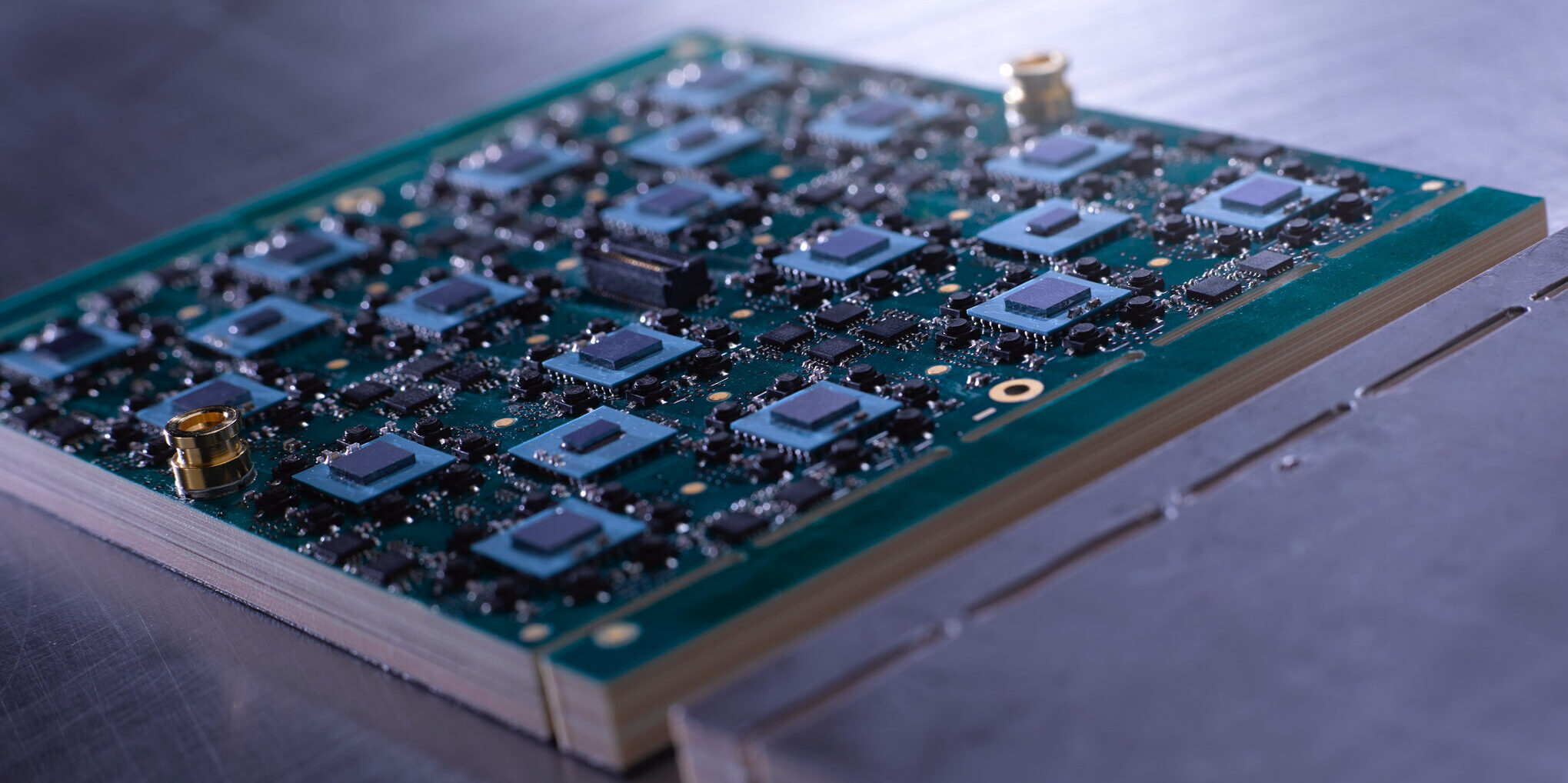
Industry: Satellite Communications/Military Radar
Application Scenario:
256-channel phased array antenna system (28GHz Ka-band)
Customer requirements: ±60° beam steering, ±0.5dB amplitude consistency, 8-week delivery
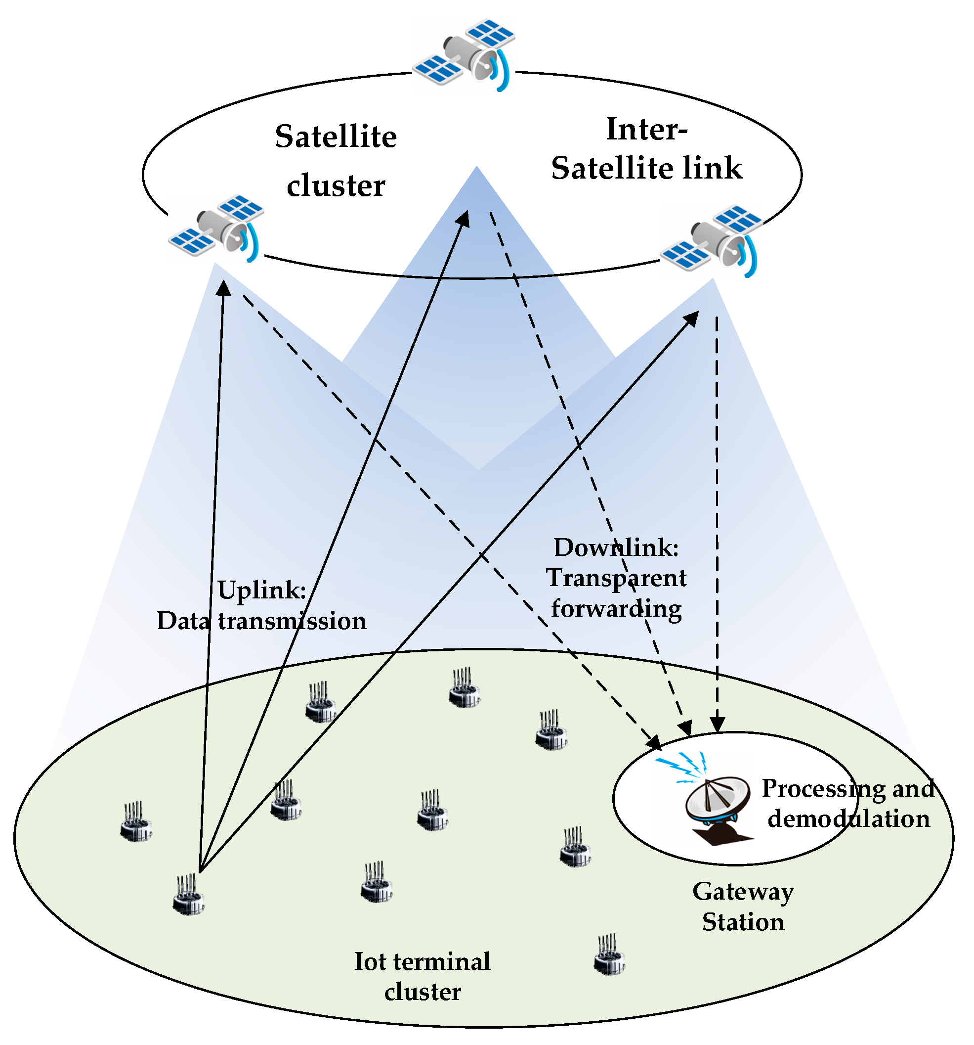
(ASTM E1647 Validated, 60% Cost Reduction vs. Ceramic Substrates) Project Introduction This project developed a mission-critical PCB for commercial satellite IoT terminals requiring: “The Rogers/Taconic hybrid stackup solved our insertion loss and CTE mismatch problems simultaneously.”— Lead RF Engineer (Client R&D Team) Key Specifications Parameter Target Achieved Frequency Range 902-928MHz (LoRa) + 1.5GHz (SatIoT) 850MHz-1.6GHz […]

1. Customer Profile Client: AnonymousIndustry: ADAS (Advanced Driver Assistance Systems), Autonomous VehiclesApplication: 77GHz Long-Range Radar (LRR) for Highway Pilot & Collision Avoidance Customer’s Requirements: Key Challenges: 2. KKPCB’s Radar PCBA Solution (A) Material & Stackup Layer Material Function Key Specs RF Layers Rogers RO3003 Antenna Array & Front-End Dk=3.0, Df=0.0013 @ 77GHz Core Arlon 25FR […]
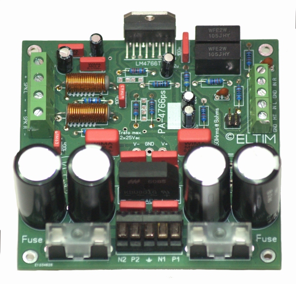
Client: A leading European audio equipment manufacturer
Industry: High-End Consumer Audio / Professional Sound Systems
Application: Stereo Power Amplifier Modules
Client: Anonymous
Industry: Telecom Infrastructure, 5G Macro/Micro Base Stations
Application: Power Amplifier (PA) Modules + RF Front-End PCBs
High-power base station equipment requiring PCBs are able to handle:
High current (30A+) for PAs
Low-loss RF (3.5GHz-28GHz for 5G)
Thermal stability (85°C ambient, 125°C local hotspots)
Key Challenges Faced:
Delamination risk from mixed thick-copper (6oz) and RF layers.
EMI coupling between power and RF sections.
Thermal warping under high thermal cycling.
Client: Anonymous
Industry: Fiber Optic Test & Measurement, High-Speed Data Transmission
Application: Next-gen 100G/400G+ optical transceivers, OTDR equipment, and 50GHz RF test modules.
FIS designs precision fiber optic tools, requiring ultra-low-loss PCBs to maintain signal integrity at millimeter-wave frequencies (up to 50GHz). Their challenges include:
Insertion loss degrading high-speed signals (>40Gbps).
Impedance mismatches causing reflection noise.
Thermal expansion leading to microvia cracking in compact designs.

The customer is a globally leading manufacturer of communication equipment, specializing in the development and production of large-scale routers, switches, servers, and high-speed networking devices. As modern network communications demand increasingly high signal integrity, reliability, and thermal stability, the customer required an 18-layer PCB with low-loss material (S1000-2M) and advanced immersion gold plating to ensure stable signal transmission and long-term reliability
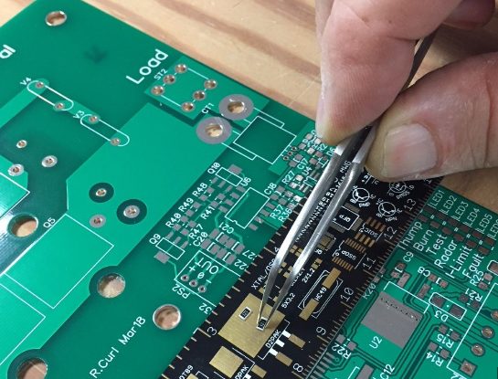
Basic soldering guide on how to solder electronic components to a printed circuit board (PCB). This is a detailed and complete soldering guide for both automated soldering in mass production and manual soldering in PCB rework and repair.
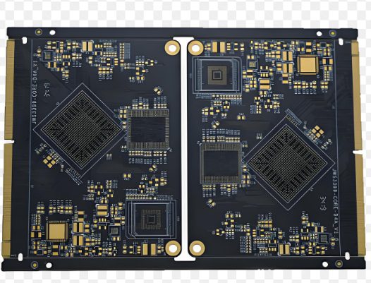
A Multilayer PCB (Printed Circuit Board) is a type of PCB with more than two conductive layers. Unlike a double-sided PCB, which has two copper layers (top and bottom), a multilayer PCB consists of three or more layers of copper, interconnected by copper-plated vias. The number of layers can range from 3 layers to 40 layers or more, depending on the design requirements