


As electronic devices become more complex and ubiquitous, the need for reliable and high-performance PCBs continues to grow. PCB testing standards provide a framework for ensuring that these essential components meet industry benchmarks for safety, reliability, and functionality. Manufacturers who adhere to these testing standards are better positioned to deliver high-quality, dependable products, build trust with their customers, and minimize the risk of product failures. Whether through visual inspection, electrical testing, or advanced X-ray analysis, rigorous testing ensures that the PCBs will perform as expected, even in the most challenging environments.
As the largest PCB manufacturer globally, China not only leads in production volume and technology but also continues to innovate. By increasing research and development investment and optimizing production processes, China’s PCB industry has gradually transitioned from low-end manufacturing to high-end production, especially excelling in areas such as high-frequency, high-speed, and high-precision applications. Meanwhile, China’s cost advantages, rich industrial chain resources, and mature supply chain management systems further solidify its dominant position in the global market.
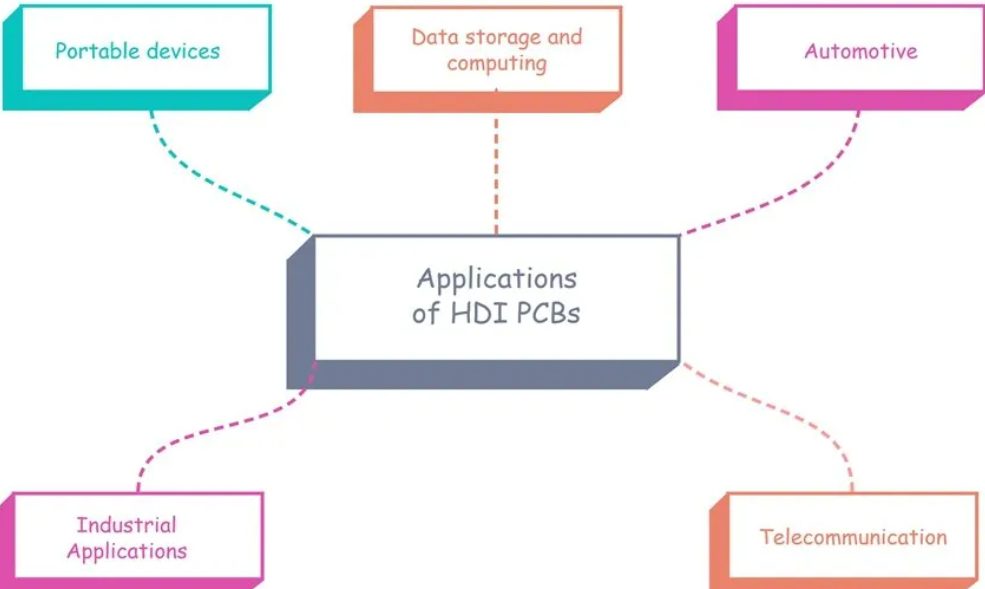
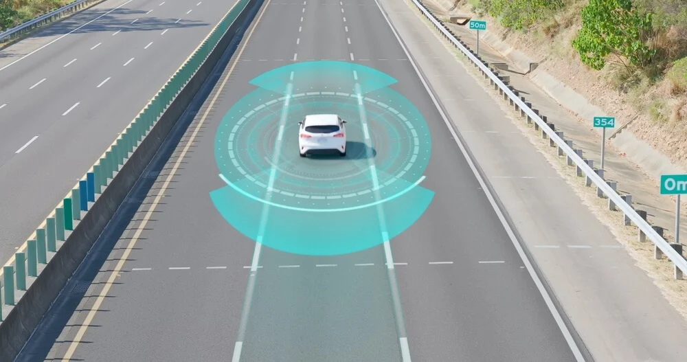
In the present world, especially in the current technological era, devices are becoming more compact and advanced. For implementing the compact and at the same time advanced electronic technology in the world, HDI PCBs contribute abundantly
In conclusion, managing EMI and ensuring EMC are critical aspects of PCB design and manufacturing. By carefully considering factors like trace routing, grounding, component selection, and shielding, designers can minimize the risks associated with electromagnetic interference and create devices that perform reliably and safely.
The Internet of Things (IoT) is revolutionizing industries worldwide, and its influence on Printed Circuit Board (PCB) design and manufacturing is profound. As IoT devices become more compact, efficient, and interconnected, the demand for innovative PCB designs has surged. This blog delves into how IoT is transforming PCB design and manufacturing, the challenges it poses, and the opportunities it presents.
When it comes to assembling Printed Circuit Boards (PCBs), there are two primary technologies: Surface Mount Technology (SMT) assembly and Through-Hole Technology (PTH) assembly
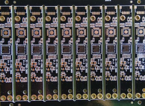
Printed Circuit Board (PCB) manufacturing is a complex process that involves multiple steps, one of which is the application of solder paste or other materials onto the board. This is often accomplished through screen printing, a technique that requires a high-quality stencil. The PCB screen printing stencil making process is a crucial part of PCB assembly, as it directly affects the quality and reliability of the final product
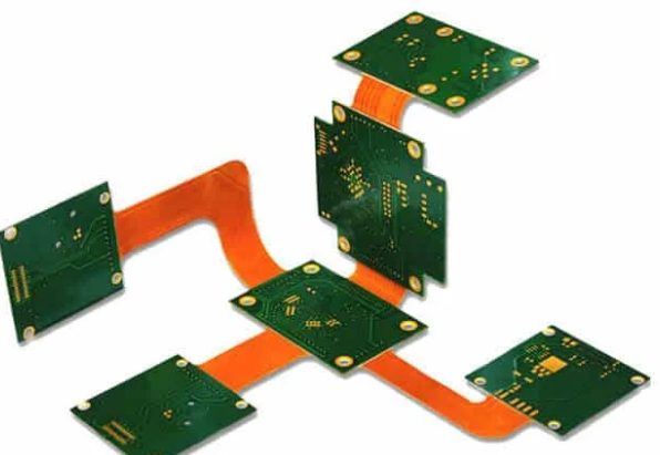
Special processing technologies are non-conventional processes used in the production of printed circuit boards to meet specific needs. These technologies usually involve high-precision, high-complexity processing requirements and are capable of processing circuit boards with special functions or properties, such as high-frequency PCBs, flexible PCBs, and high-density interconnect (HDI) boards.
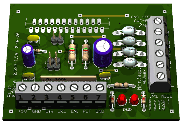
A motor controller is an electronic or electrical device used to regulate the speed, torque, and position of a motor. It can automatically or manually start, stop, and protect the motor from issues like overloads.
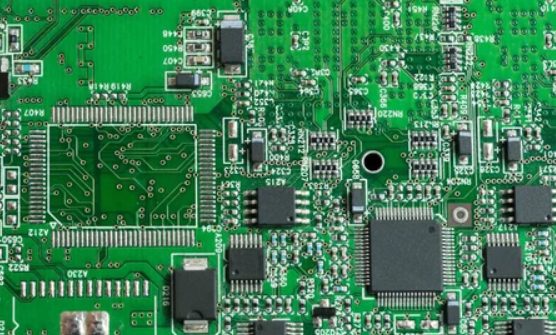
Printed circuit boards (PCBs), or called printed wiring boards (PWBs), have become basic parts in almost all areas of modern technologies. Copper trace is a crucial element on circuit boards. The copper always plays a role of carrying electrical signals to different components across the board assembly. Without traces, the PCB will not function. Of all the elements that build PCB boards, copper is one of the most important.