


Customized PCBA Manufacturing Solution for a Data Transmission Module
1. Background Overview
A European industrial automation customer required a high-reliability data transmission module for use in rugged and space-constrained environments. The module needed to meet strict requirements for signal integrity, power efficiency, and heat dissipation, while ensuring fast production and stable long-term performance.
2. Application Scenario
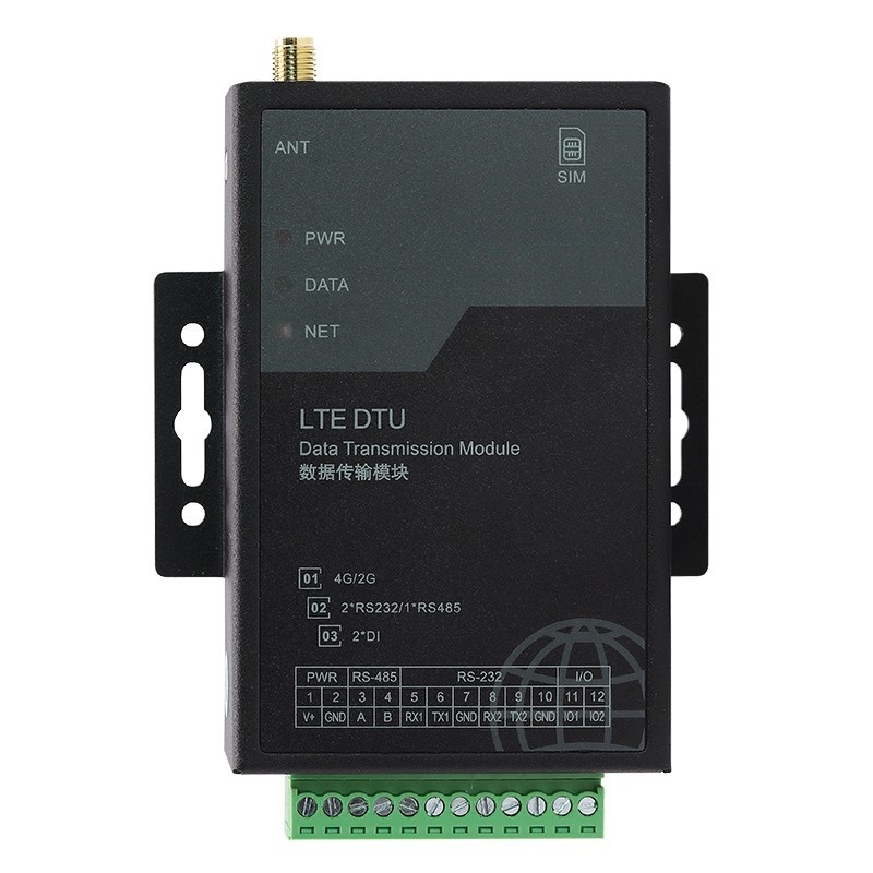
The PCBA is used in real-time data transmission within an industrial control system, where stable communication between subsystems is critical. Applications include smart factories, process control, and remote device monitoring.

3. Key Product Parameters
| Parameter | Specification |
|---|---|
| Transmission Standard | RS-232 / RS-485 / TTL |
| Baud Rate | 300bps – 921600bps |
| Operating Voltage | 3.3V / 5V |
| Isolation Voltage | 2500V |
| Dimensions | 45mm x 25mm |
| Operating Temperature Range | -40°C to +85°C |
| PCB Layers | 4-layer high-density design |
| EMI/EMC Protection | Integrated filtering & shielding |
4. Application Results
After implementing KKPCB’s PCBA manufacturing solution:
- Defect rate decreased by 45%, improving communication reliability in harsh environments
- Overall cost reduced by 15% through optimized layout and panelization
- Signal integrity improved by 30%, thanks to impedance-controlled multilayer PCB stack-up
- Lead time shortened by 22%, from 4.5 weeks to 3.5 weeks
5. KKPCB Advantages in This Case
KKPCB leveraged its expertise in high-reliability PCB fabrication and precision SMT assembly. Our IPC-A-610 Class 2/3 quality control standards, AOI+X-ray full-process inspection, and in-house engineering team enabled us to meet the customer’s strict electrical and mechanical specifications while ensuring consistency across batches. Our MES system also helped track production status in real-time.
6. KKPCB’s Manufacturing-Focused Custom Solution
Based on the customer’s needs for strong EMI performance and thermal management in a compact footprint, KKPCB provided:
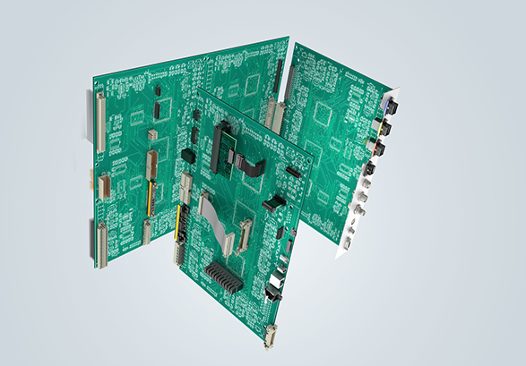
- Customized 4-layer PCB with impedance control, suitable for high-speed data transmission
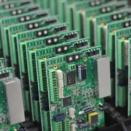
- Miniaturized SMT placement with 01005 and fine-pitch IC handling, enabling compact design
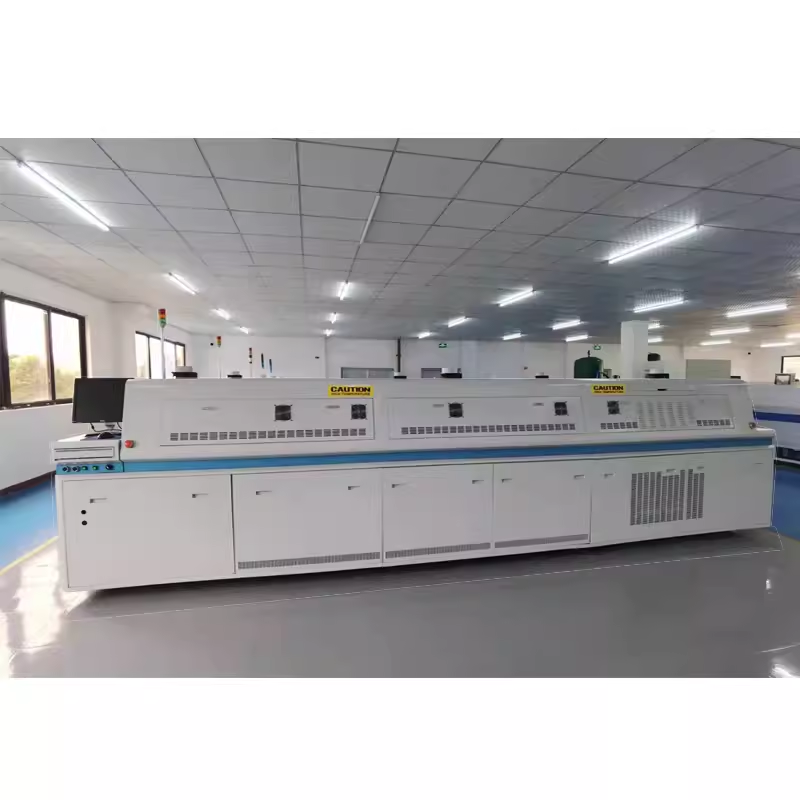
- Enhanced solder joint quality using nitrogen reflow soldering and automatic paste inspection
- Panelized PCB layout optimization, reducing material usage and increasing assembly efficiency
- DFM suggestions, helping the client avoid costly design mistakes and improving long-term maintainability
7. Real-World Impact
Our PCBA solution enhanced the stability of the customer’s industrial communication system. The error rate in signal transmission dropped by 37%, while thermal performance improved by 20%, allowing the product to operate longer without additional cooling. Additionally, the improved process design resulted in a 25% increase in first-pass yield and significant savings on warranty returns.