



How to design high frequency PCB for microwave circuit
High-frequency PCB design treats traces, reference planes and transitions as parts of the circuit. For microwave applications, a connection that looks simple on a schematic can introduce loss, reflections or unwanted coupling on the finished board. This guide presents seven practical checks for planning a high frequency PCB before fabrication.
Contents
1. Select materials for high-frequency PCB design
Start with the operating frequency, bandwidth, insertion-loss budget and environmental requirements. Compare dielectric constant, dissipation factor, copper profile and material thickness using the laminate supplier’s documentation. Values measured under different test methods are not always directly comparable.
A material suitable for a short RF connection may not suit a long transmission line with a tighter loss budget. Consider fabrication availability, dimensional stability and assembly requirements alongside electrical properties. Avoid selecting a laminate solely because its nominal dielectric constant appears attractive.
2. Agree on the stackup before routing
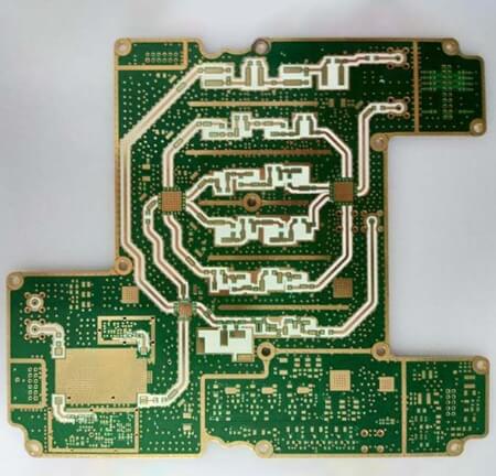
Discuss the proposed layer structure with the fabricator early. Trace width, dielectric thickness, copper thickness and the reference plane all affect controlled impedance. A trace width calculated for one stackup should not be transferred to another without checking it.
Identify the transmission-line structure used by each critical net. Microstrip and stripline have different field distributions and manufacturing considerations. Record the impedance target and tolerance on the fabrication drawing, then confirm how the supplier will verify them.
3. Maintain continuous return paths
High-frequency PCB design needs a clear reference plane. Avoid crossing plane splits with critical signals, because a disrupted return path can increase coupling and radiation. Place return-path transitions near signal-layer transitions where the design requires them.
Keep RF routes direct and assess bends, pads, connector launches and vias as discontinuities. A short route is helpful, but length alone does not guarantee good performance. The complete path between components should be reviewed against the intended frequency range.
4. Control coupling between circuit sections
Separate sensitive receive paths from strong transmit signals, switching power supplies and noisy digital interfaces. Determine spacing from the stackup and coupling requirements rather than applying one universal clearance rule. Keep reference planes intact while planning functional placement.
Review the placement of decoupling capacitors and the associated connections. Long connections can limit their usefulness at higher frequencies. Follow component reference designs where appropriate, while checking whether their board stackup matches the planned implementation.
5. Check connectors, vias and assembly details
Connector launches and component pads can dominate performance even when the transmission line itself is well designed. Include relevant package and connector models in the review. Consider via stubs and transitions when determining whether additional analysis or fabrication processes are needed.
Confirm solder-mask assumptions, finish requirements and component assembly constraints with the supplier. Manufacturing notes should distinguish required performance from optional process preferences. This helps prevent an electrical assumption from being lost during quotation or production.
6. Verify the design with appropriate models
Use suitable field-solving or electromagnetic simulation tools for critical structures. Include realistic material properties and geometry. Check the sensitivity to manufacturing tolerances instead of relying only on a nominal simulation result.
Plan prototype measurements around the actual acceptance criteria. Document the test fixtures, calibration approach and frequency range so that measurements can be compared meaningfully with the model. Investigate discrepancies before committing to a larger production run.
7. Complete the high-frequency PCB design release checklist
- Confirm laminate and stackup availability.
- Specify controlled-impedance targets and tolerances.
- Review reference-plane continuity and transitions.
- Check isolation between sensitive and noisy circuits.
- Review connector launches, pads and via structures.
- Confirm fabrication and assembly notes.
- Define prototype measurement and acceptance criteria.
For additional background, consult the application resources available from Rogers Advanced Electronics Solutions and compare them with the selected material’s current data sheet. Discuss the project with KKPCB before finalizing fabrication files.
Frequently asked questions
Is every fast digital board a microwave board?
No. Digital edge rates can introduce high-frequency behavior, but the analysis and acceptance criteria depend on the signals and interconnects involved. Evaluate the relevant spectrum and geometry rather than classifying a board from clock frequency alone.
Can a better laminate fix every RF problem?
No. Material selection is only one part of high-frequency PCB design. Return-path interruptions, mismatched transitions and coupling can still limit performance. Review the entire signal path before changing materials.
