




HDI PCB Design Checklist: 7 Checks Before Fabrication
This HDI PCB design checklist is useful when component pitch and routing density exceed what a conventional through-hole stackup can handle within the available board area. Microvias and sequential build-up layers can create routing room, but they also add fabrication steps and reliability questions. Before layout starts, agree on the stackup, via structure, trace and gap limits, and inspection plan with the manufacturer. This HDI PCB design checklist is intended for engineers preparing an HDI board for fabrication.
1. Confirm why the design needs HDI
Identify the BGA pitch, pin count, escape-routing demand, board outline, layer limit, and signal-integrity targets. Do not add microvias simply because the product is compact. Compare a conventional multilayer option with an HDI PCB stackup and document which nets or component regions require the extra density. This makes cost and reliability tradeoffs easier to review.
2. Choose the build-up stackup before routing
Specify the core, build-up layers, dielectric thicknesses, copper weights, and reference planes. A one-step or two-step build-up has different processing and cost implications. Keep critical signal routes close to appropriate reference planes, and check the return path at every layer transition. The final stackup should reflect the fabricator’s available materials and lamination process. See KKPCB’s multilayer PCB overview for related construction choices.
3. Define the microvia architecture
List each blind, buried, and through-via layer pair and decide whether microvias will be staggered or stacked. Stacked microvias need a suitable filled and capped landing structure and can have greater fabrication and reliability demands. Avoid assuming that a via diameter or stack count is universally safe. Confirm drill depth, pad size, aspect ratio, capture land, via fill, and registration with the fabricator. Altium’s via-type documentation explains the layer connections; an IPC paper on microvia failure modes discusses reliability considerations.
4. Set trace, gap, and pad rules from capability data
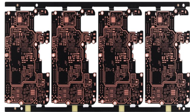
Use the fabricator’s minimum trace width, spacing, drill-to-copper clearance, and registration capability as design-rule inputs. Check both the nominal geometry and the tolerance after etching and lamination. Fine-pitch fanout should also be reviewed with assembly pad and solder-mask requirements. Altium’s HDI design-rule guide recommends deriving these constraints from the chosen fabricator rather than reusing settings from another board.
5. Protect signal and power integrity
Shorter interconnects can help a dense design, but HDI alone does not guarantee better electrical performance. Model controlled impedance using the actual dielectric and finished copper dimensions. Review reference-plane continuity, via transitions, return paths, and power distribution. If high-frequency signals share the board, coordinate the HDI stackup with the high-frequency PCB material and loss requirements. Rogers also discusses multilayer RF material choices for compact designs.
6. Plan manufacturing and inspection together
Sequential lamination, laser drilling, plating, and microvia filling create multiple process checkpoints. Ask how the fabricator will inspect layer registration, via fill, plating continuity, and finished dimensions. For high-reliability applications, define appropriate coupon, thermal-stress, and electrical-test requirements before production. Use the HDI PCB design checklist to confirm that the test plan matches the via architecture and the end-use environment, not merely the number of layers.
7. Send a complete HDI RFQ package
A complete HDI PCB design checklist package includes Gerber or ODB++ data, drill and via tables, proposed stackup, material choices, finished copper thickness, controlled-impedance targets, smallest trace and gap, board outline, quantities, surface finish, and inspection needs. Mark any via-in-pad and stacked microvia locations explicitly. KKPCB can review the supplied design against its current HDI manufacturing capabilities and discuss a prototype plan. Send the files to request an HDI PCB quotation.
Frequently asked questions
Does every HDI PCB require stacked microvias?
No. The routing and layer-pair requirements determine whether staggered vias or another construction can meet the design. Review reliability and cost with the fabricator.
When should the stackup be agreed?
Before detailed routing. The dielectric thickness, copper weight, reference planes, and microvia layer pairs determine many of the design rules.
