







Microwave PCB Design Issues: 7 Ways to Avoid RF Failures
Microwave PCB design issues usually appear when a layout that works at lower frequencies is treated like an ordinary digital board. At RF and microwave frequencies, a trace is a transmission line, every reference-plane break changes the return path, and small changes in copper geometry can shift impedance. The safest approach is to define the stackup, materials, impedance targets, launches, test method, and fabrication tolerances before routing begins.
What causes microwave PCB design issues?
The main causes are impedance discontinuities, excessive dielectric or conductor loss, poor return-current continuity, unwanted coupling, resonant structures, and uncontrolled manufacturing variation. These effects become more important as electrical length increases relative to wavelength. A board can pass a schematic review and still fail insertion-loss, return-loss, phase, or radiated-emissions targets because the physical interconnect was not designed as part of the circuit.
The following seven practices address the most common microwave PCB design issues while keeping the design manufacturable.
1. Freeze the material and stackup before routing
Do not calculate a controlled-impedance line from a generic dielectric constant. Use the laminate supplier’s design Dk at a relevant frequency and confirm the finished dielectric thickness, copper thickness, copper profile, solder-mask condition, and fabrication tolerance with the PCB manufacturer. Rogers explains that substrate thickness, copper thickness, conductor width, Dk, moisture, and copper roughness can all influence high-frequency impedance. Review our PCB materials options and discuss the intended construction before final layout.
2. Control transmission-line geometry and reference continuity
Define whether each critical net uses microstrip, stripline, grounded coplanar waveguide, or another verified structure. Maintain the calculated trace width and gap, avoid neck-down sections unless they are modeled, and keep a continuous reference plane directly adjacent to the signal. Never route an RF line across a split, void, or plane edge. If the return current must change layers, place stitching vias close to the signal transition so the return path remains short and predictable.
A nominal 50-ohm target is common, but it is not universal. The correct impedance comes from the RF architecture, component ports, connectors, and measurement environment. Include an impedance table in the fabrication notes and request suitable coupons when impedance verification is required.
3. Model bends, vias, pads, and connector launches
Many microwave PCB design issues originate at discontinuities, which are often more damaging than a long uniform trace. Avoid sharp geometry changes and keep bends smooth or mitered according to an evaluated model. A via transition adds inductance and capacitance; its unused barrel can form a stub. At higher frequencies, optimize the via diameter, pad, antipad, ground-via pattern, layer transition, and backdrill depth when backdrilling is justified.
Connector launches deserve the same attention. Model the transition from the coaxial or board connector into the selected PCB transmission-line structure. Keep the launch reference geometry consistent with the connector supplier’s recommendation and validate any footprint changes rather than copying a generic land pattern.
4. Manage coupling, grounding, and resonance
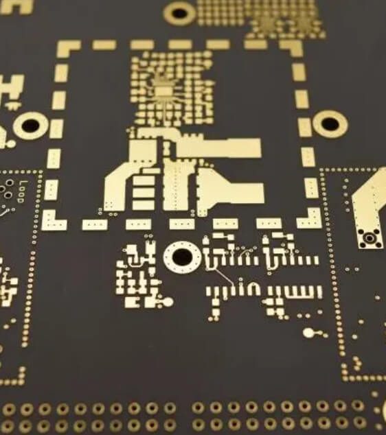
Separate sensitive receive paths from power amplifiers, clocks, switching regulators, and fast digital interfaces. Coupling depends on frequency, spacing, parallel length, reference geometry, and field containment, so a single universal spacing rule is not reliable. Use grounded shielding structures only when their via pitch and enclosure geometry have been checked for the operating band. Poorly designed via fences, cavities, and plane openings can create resonances instead of solving them.
5. Include fabrication effects in the loss budget
Loss-related microwave PCB design issues become more serious at higher frequencies. Insertion loss is affected by dielectric dissipation factor, copper conductivity, surface roughness, trace geometry, and surface finish. Solder mask over a microstrip changes the effective dielectric environment and may shift impedance or loss. Confirm whether critical RF traces should be masked or exposed, and specify the requirement clearly. Choose a finish that meets assembly, shelf-life, bondability, corrosion, and RF performance needs rather than selecting it from cost alone.
6. Simulate the real geometry, not an ideal schematic
Use a field solver or electromagnetic simulation for critical interconnects, especially launches, filters, coupled structures, dense transitions, and high-frequency via fields. The model should include the intended material data, finished copper, actual dielectric thicknesses, reference planes, pads, antipads, and connectors. Run sensitivity checks across reasonable manufacturing tolerances so the design is not optimized only for nominal dimensions.
7. Plan measurement and de-embedding before fabrication
Verification-related microwave PCB design issues are easier to diagnose when measurement is planned early. Decide how the board will be verified before the layout is released. A TDR can locate impedance discontinuities along a transmission path, while a vector network analyzer can characterize S-parameters such as insertion loss and return loss. Keysight notes that fixture effects may need to be removed so the measurement reference plane is moved to the device plane. Provide calibration, thru/reflect/line, or de-embedding structures when the test strategy requires them.
For a standards-based design review, consult IPC-2228, Sectional Design Standard for High Frequency (RF/Microwave) Printed Boards. IPC specifically recommends early dialogue among the designer, material supplier, and an experienced fabricator.
RF PCB design review checklist
- Operating frequency range, bandwidth, power, and temperature are defined.
- The stackup names exact materials, finished dielectric thicknesses, copper weights, and roughness assumptions.
- Every controlled-impedance structure has a target and tolerance.
- Reference planes remain continuous under critical routes.
- Vias, stubs, bends, pads, antipads, and connector launches are modeled where necessary.
- Isolation, grounding, shielding, and thermal paths are reviewed together.
- Surface finish and solder-mask conditions are specified for critical RF lines.
- Fabrication coupons, VNA/TDR structures, and acceptance criteria are documented.
How KKPCB helps prevent microwave PCB design issues
KKPCB supports high-frequency PCB fabrication, controlled-impedance review, multilayer stackup coordination, and DFM feedback. Our engineering review can flag ambiguous material calls, unrealistic tolerances, discontinuous reference paths, difficult via structures, and missing test requirements before production. For complex mixed-signal projects, also review our PCB layout services and multilayer PCB capabilities.
To receive a useful quotation, send the Gerber or ODB++ data, drill files, stackup, material specification, finished copper, impedance table, surface finish, solder-mask requirement, quantity, and test criteria. Request an RF PCB review and quotation to resolve potential microwave PCB design issues before fabrication.
