





Multilayer PCB Manufacturing Challenges: 8 Critical Controls
Multilayer PCB manufacturing challenges increase quickly as layer count, routing density, aspect ratio, copper weight, and impedance requirements rise. Reliable production is not simply a matter of pressing more copper layers together. It requires coordinated control of material behavior, inner-layer imaging, registration, lamination, drilling, plating, inspection, and electrical test.
This guide explains the eight most important process controls for engineers sourcing complex multilayer boards. It also shows which fabrication data KKPCB needs to evaluate manufacturability before tooling.
What makes multilayer PCB manufacturing difficult?
A multilayer PCB contains three or more conductive circuit layers separated by dielectric material. In production, manufacturers commonly describe boards with four or more layers as multilayer boards. The technical risk, however, depends on the complete design rather than layer count alone. A 10-layer board with generous features can be easier to build than a 6-layer board with thin dielectrics, stacked microvias, heavy copper, and a demanding impedance tolerance.
The main multilayer PCB manufacturing challenges arise because every process affects the next one. Inner-layer movement changes registration. Resin flow changes dielectric thickness and impedance. Drilling quality affects desmear and hole-wall plating. Copper plating changes finished hole size and trace geometry. A capable fabricator therefore reviews the complete stackup, drill structure, material system, artwork, and reliability requirements as one connected process.
1. Material selection and compatibility
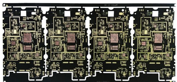
Solving multilayer PCB manufacturing challenges begins with the material system. Core and prepreg materials must support the assembly temperature, electrical performance, mechanical reliability, copper weight, and drilling process. Important properties include glass-transition temperature, decomposition temperature, Z-axis expansion, dielectric constant, dissipation factor, moisture absorption, resin content, and copper-foil profile. High-speed or RF layers may need low-loss laminates, while power sections may need heavier copper and greater resin fill. Rogers Advanced Electronics Solutions publishes technical resources for high-frequency laminate selection.
Mixing material families without qualification can create different expansion rates, weak interfaces, unpredictable resin flow, or unreliable plated holes. The stackup should identify the exact laminate family, core thickness, prepreg style, copper weight, and finished dielectric targets. KKPCB reviews these items against the intended assembly cycles and application environment before production. See our PCB materials guide for common substrate options.
2. Inner-layer imaging and etching
Fine lines, small clearances, dense BGA escape routing, and heavy copper make inner-layer imaging more sensitive. Photoresist coating, exposure energy, developer condition, etchant chemistry, and copper thickness must remain controlled to prevent opens, shorts, neck-down, and excessive undercut. Laser direct imaging can improve artwork registration and feature definition, but it does not replace process compensation or inspection.
Each completed inner layer should be inspected by automated optical inspection before lamination. Defects trapped inside a pressed panel cannot be repaired economically. Coupon measurements and first-article data help confirm that the etched trace width will meet the impedance model after plating and final processing.
3. Interlayer registration
Registration is one of the most visible multilayer PCB manufacturing challenges. Thin cores expand and contract during oxide treatment, imaging, etching, and lamination. The movement is not always identical in the machine and transverse directions. Large panels, asymmetric copper distribution, and mixed materials make compensation harder.
Manufacturers use tooling holes, optical targets, X-ray registration, pin lamination, riveting, or fusion bonding according to the product structure. Scale factors should be based on measured process history for the selected material and copper distribution. Designers can improve yield by using practical annular rings, balanced copper, clear layer orientation marks, and unambiguous drill-to-copper requirements.
4. Lamination and resin flow
Among multilayer PCB manufacturing challenges, lamination requires especially close control. During lamination, heat and pressure cause prepreg resin to flow, fill copper-free areas, cure, and bond the stack. Insufficient resin can cause voids or poor fill around thick copper. Excessive flow can reduce dielectric thickness or create resin starvation in other areas. Incorrect heating rate, pressure timing, vacuum, or cure time can contribute to delamination, layer shift, thickness variation, or trapped air.
The press cycle must match the resin system, panel construction, copper distribution, and total mass. Sequential lamination for blind and buried vias adds extra thermal cycles and requires a defined buildup sequence. A symmetric stackup and balanced copper distribution reduce bow and twist, but the finished board still needs dimensional and flatness verification.
5. Controlled impedance and dielectric thickness
Controlled impedance depends on trace geometry, copper thickness, dielectric thickness, dielectric properties, solder mask, and the reference-plane structure. The laminate data-sheet dielectric constant is not automatically the correct value for every field solver or frequency. Fabricators normally use validated process values and finished-copper assumptions when creating the impedance model.
Provide target impedance, tolerance, layer, trace type, reference plane, and test-coupon requirements. Do not lock line width and spacing before the stackup is reviewed unless those dimensions are mandatory. KKPCB can adjust manufacturable geometry during PCB layout and stackup review and confirm it with time-domain reflectometry coupons where required.
6. Drilling, desmear, and hole geometry
Thick panels and small holes increase drill aspect ratio, tool wear, heat, smear, hole-wall roughness, and positional error. Glass weave and copper interfaces can deflect small drills. Poor drilling or an unsuitable desmear cycle can leave resin on exposed inner-layer copper, weakening the electrical connection after plating.
Finished hole size, drill size, panel thickness, copper plating allowance, and aspect ratio must be evaluated together. Small vias may require reduced stack height, optimized feeds and speeds, controlled hit count, and new drill tools. Laser-drilled microvias need separate controls for capture-pad alignment, dielectric removal, copper preparation, filling, and sequential buildup. The official IPC-2221B table of contents identifies the standard’s coverage of holes, vias, test coupons, and design considerations.
7. Copper plating and interconnect reliability
After hole preparation, electroless copper creates a conductive seed layer and electrolytic plating builds the required copper thickness. Deep, narrow holes are difficult because solution exchange and current distribution are less uniform through the barrel. The process must provide adequate copper at the hole center without excessive surface plating.
Reliability checks may include microsection analysis, plating-thickness measurement, thermal stress, continuity, and resistance monitoring. High-aspect-ratio through holes, stacked microvias, via-in-pad structures, and repeated lead-free assembly cycles deserve special review. Acceptance criteria must be stated on the fabrication drawing or purchase specification; they should not be inferred from a generic board description.
8. Inspection, electrical test, and traceability
Managing multilayer PCB manufacturing challenges requires inspection throughout the route. Inspection should be built into the route, not left until final shipment. Useful controls include incoming material verification, inner-layer AOI, registration measurement, press thickness checks, X-ray analysis, drill inspection, plated-hole microsections, solder-mask inspection, impedance testing, and 100% electrical test. Flying-probe testing is flexible for prototypes; fixture testing can be efficient for higher volumes.
Material lot, process route, inspection result, and nonconformance disposition should be traceable. For high-reliability products, agree on coupon design, test frequency, reports, and retention samples before production. KKPCB’s quality-control process links these inspections to the manufacturing traveler and customer requirements.
DFM checklist for complex multilayer boards
- Provide Gerber, ODB++, or IPC-2581 data with a complete NC drill package.
- Include the layer order, finished thickness, copper weights, and approved material or performance class.
- Identify controlled-impedance nets, targets, tolerances, and coupon needs.
- Separate plated, non-plated, blind, buried, and laser-drilled holes.
- State minimum finished hole size and any maximum aspect-ratio restriction.
- Define surface finish, solder-mask type and color, via fill, edge plating, and special processes.
- Specify applicable acceptance class, electrical test, reliability test, and reporting requirements.
- Supply quantity, panelization constraints, assembly profile, and operating environment.
How KKPCB controls multilayer PCB manufacturing challenges
KKPCB performs stackup and DFM review before tooling, then assigns material, registration, lamination, drilling, plating, inspection, and test controls to the production route. Our multilayer PCB manufacturing capability supports prototypes and production boards with controlled impedance, blind and buried vias, HDI structures, high-frequency materials, heavy copper, and rigid-flex constructions.
To evaluate your project’s multilayer PCB manufacturing challenges, send the fabrication package, stackup, material requirements, finished thickness, copper weight, via structure, impedance table, surface finish, acceptance criteria, quantity, and target delivery date. Request a KKPCB DFM review and RFQ before freezing the design.
