


Choose the right PCB surface treatment for longer service life
PCB surface treatment, also called a PCB surface finish, protects exposed copper and creates the interface for soldering, contact, or wire bonding. The right finish depends on the assembly method, pad pitch, storage conditions, operating environment, and, for RF boards, the effect of plating on signal loss. There is no single finish that is best for every design.
How to choose a PCB surface treatment
Start with the finished board’s actual requirements. Are the pads for fine-pitch SMT, repeated connector contact, or wire bonding? How many reflow cycles are expected? How long will bare boards be stored before assembly, and under what packaging conditions? For a high-frequency PCB, also identify the transmission-line geometry and acceptable insertion loss. Ask the fabricator to confirm finish availability, thickness control, and inspection requirements for the selected stackup.
ENIG: flat solderable pads, with an RF tradeoff
Electroless nickel immersion gold (ENIG) gives a relatively flat, solderable surface that is widely used for fine-pitch assembly. The gold protects the nickel before soldering; the nickel is the barrier layer over copper. On exposed RF transmission lines, however, nickel can increase conductor loss compared with bare copper or some thin alternative finishes. The size of that effect depends on frequency, line geometry, and the plating process. Rogers explains the frequency-dependent loss mechanism in its technical paper on high-frequency PCB losses. Do not reject ENIG automatically: decide whether the critical RF traces are finished, and verify the modeled and measured loss budget.
ENEPIG: consider soldering and wire bonding together
Electroless nickel electroless palladium immersion gold (ENEPIG) adds a palladium layer between nickel and gold. It is a candidate when a board needs both solderable pads and specified wire-bonding performance. The exact bond type, assembly process, deposit thickness, and qualification plan still matter. ENEPIG is a multi-step process, so confirm capability and cost before choosing it. IPC’s surface-finish comparison lists its benefits and process limitations.
OSP, immersion silver, and immersion tin
Organic solderability preservative (OSP) forms a thin protective layer on copper and leaves a flat surface for assembly. Its storage, handling, and reflow limits depend on the product and process, so agree on the assembly schedule with the supplier. Immersion silver and immersion tin are also flat finishes. Their handling and storage controls deserve attention because surface condition can change before assembly. For a low-loss RF design, these options may be worth evaluating against ENIG, but solderability, shelf life, and the planned manufacturing flow must be checked together. Rogers discusses finish selection for millimeter-wave circuits.
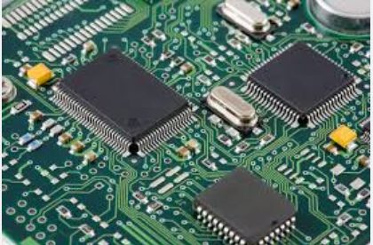
HASL and hard gold serve different needs
Hot air solder leveling (HASL), including lead-free HASL, provides a solderable coating, but its surface flatness can be a problem for very fine-pitch pads. Electrolytic hard gold is typically considered for contact areas such as edge fingers that face repeated mating or wear. It should not be treated as a general substitute for a solderable finish across the whole board. If a design combines contact fingers and solder pads, specify the finish by feature and ask the fabricator to confirm the selective-plating process.
A practical decision checklist
- Assembly: pad pitch, component types, solder alloy, reflow count, and any wire bonds.
- Electrical: RF frequency, transmission-line type, loss budget, and which copper features receive finish.
- Reliability: expected storage period, packaging, exposure, and contact wear.
- Fabrication: finish thickness, process capability, inspection standard, lead time, and cost.
When choosing a PCB surface treatment for PCB and PCBA projects, review the finish along with the laminate selection and assembly process. KKPCB can assess the manufacturability of a proposed finish against your board and assembly requirements. To request a quotation, send Gerber or ODB++ files, stackup, material, finish, quantity, critical pad or RF features, and any test requirements through the KKPCB contact page.
Frequently asked questions
Which PCB surface treatment is best for fine-pitch SMT?
A flat finish such as ENIG, ENEPIG, OSP, immersion silver, or immersion tin may be considered. The choice depends on assembly timing, reliability needs, and fabricator capability.
Does ENIG always cause unacceptable RF loss?
No. Nickel can add loss on an exposed RF line, but whether that matters depends on the specific frequency, geometry, finish coverage, and loss budget. Model and measure the critical path.
