






Single-Layer or Double-Layer PCB: 7 Reliable Checks
A single-layer or double-layer PCB can often be identified by examining the copper pattern, plated holes, and manufacturing files. However, solder mask, components, conformal coating, and internal copper can hide important details. The most reliable method is to combine visual inspection with the Gerber data, drill files, and fabrication drawing rather than relying on board color or component placement alone.
How to identify a single-layer or double-layer PCB
A single-layer board has one conductive copper layer on one side of an insulating base material. A double-layer board has two conductive copper layers, one on each side of the insulating core. IPC technical material describes a single-sided board as having interconnect metallization on one side only, while a double-sided board has metal interconnects on both sides. Double-sided designs commonly use plated through-holes or vias to connect the two copper layers.
Component placement does not determine the copper-layer count. A single-sided PCB may have through-hole components inserted from one side and solder joints on the copper side. A double-sided PCB may place components on one or both sides. The correct classification is based on conductive circuit layers, not the number of assembly sides.
1. Inspect traces and pads on both surfaces
When inspecting a single-layer or double-layer PCB, use good lighting and magnification to look for routed copper traces, SMD pads, test pads, and copper pours on the top and bottom. If functional conductor patterns are visible on only one surface, the board may be single-layer. If independent routed traces appear on both surfaces, it is at least double-layer.
Do not confuse silkscreen graphics with copper. Silkscreen normally shows reference designators, polarity marks, logos, and outlines. Solder mask is also not a conductor layer; it is the protective coating over copper. Exposed gold, tin, or copper at pads and vias gives the clearest visual evidence.
2. Look for plated through-holes and vias
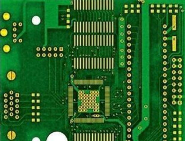
Small vias that terminate in annular rings on both sides are strong evidence of a double-layer or multilayer PCB. Their copper-plated barrels provide electrical connections between layers. Altium’s pad and via documentation explains that a through-hole pad has a barrel-shaped body formed when the drilled hole is plated during fabrication.
This check is not absolute. A single-sided board can have non-plated mounting holes or component lead holes, while some simple double-sided boards can use wire links or eyelets instead of conventional plated vias. Large component leads can also obscure the hole wall, so inspect unused holes or test vias where possible.
3. Use continuity testing carefully
With the board unpowered and safely discharged, a multimeter can test whether a top-side pad is electrically connected to a bottom-side pad through a via or plated through-hole. This can confirm an interlayer connection, but it cannot prove the total layer count. Components, solder joints, and parallel circuit paths can create continuity through the assembled circuit, so use the schematic or bare-board netlist to interpret measurements.
4. Check the board edge, but understand the limitation
A clean cross-section may reveal copper on the two outer surfaces of an uncoated sample. On a thick multilayer board, internal copper planes may sometimes be visible at an exposed edge. In normal production, routed edges, mask, resin smear, plating, or edge metallization can hide these clues. Never grind or cut a functional board simply to identify its construction; cross-sectioning is a destructive laboratory method.
5. Review Gerber and ODB++ layer names
For a single-layer or double-layer PCB, manufacturing data is more reliable than appearance. A single-layer design normally contains one copper image, such as Bottom Copper. A double-layer design contains Top Copper and Bottom Copper. Common Gerber naming varies by CAD system, so verify file attributes instead of assuming that every file beginning with “G” is copper.
- Top copper may be labeled GTL, L1, Top, or Copper_Top.
- Bottom copper may be labeled GBL, L2, Bottom, or Copper_Bottom.
- Solder mask, silkscreen, paste, profile, and drill files do not count as conductive circuit layers.
- ODB++ or IPC-2581 packages usually identify layer type and stack order directly.
Open the data in a trusted CAM viewer and toggle each copper layer. KKPCB’s PCB layout service can also review layer definitions and output a complete fabrication package.
6. Confirm plated and non-plated drill data
Excellon or NC drill files often separate plated holes from non-plated holes. A double-layer board with vias normally has plated drill data and annular pads on both copper layers. Non-plated mechanical holes alone do not indicate a second copper layer. Check the drill legend, tool table, and fabrication notes for PTH, NPTH, finished hole size, and plating requirements.
7. Read the stackup and fabrication drawing
The stackup is the authoritative description of whether a design is a single-layer or double-layer PCB, or a multilayer board. A simple single-layer stackup lists one copper foil bonded to a dielectric substrate. A double-layer stackup lists copper on both sides of a core. If internal copper layers are present, the board is multilayer even when only the outer surfaces are visible.
Look for notes such as “2-layer,” “double-sided PTH,” finished thickness, copper weight, laminate grade, impedance requirements, and surface finish. When the documentation is missing or inconsistent, ask the original designer or fabricator before generating replacement tooling.
Common identification mistakes
- Counting component sides: components on both sides do not automatically mean two copper layers.
- Counting mask colors: green coating on both sides is not proof of double-sided copper.
- Assuming every hole is a via: mounting holes and some component holes may be non-plated.
- Calling every two-sided board “two-layer”: a multilayer PCB also has copper on both outer surfaces.
- Trusting file names only: verify copper layer attributes and visible geometry in CAM data.
Single-layer or double-layer PCB selection guide
Choosing a single-layer or double-layer PCB starts with routing density and electrical needs. A single-layer board suits simple, low-density circuits where routing, electrical performance, and assembly requirements fit one conductor layer. It can reduce tooling steps and simplify inspection. A double-layer board supports higher routing density, shorter connections, better use of ground and power copper, and more flexible component placement, but requires alignment and interlayer connection control.
For dense routing, high-speed interfaces, controlled impedance, EMI control, or dedicated plane requirements, a multilayer PCB may be more appropriate. Choose the layer count from electrical and manufacturing needs, not from a simple cost target.
How KKPCB verifies PCB layer count
KKPCB reviews the copper data, drill files, netlist, board outline, stackup, and fabrication notes before production. Our DFM process checks whether the declared single-layer or double-layer PCB construction matches the supplied files, whether vias are properly defined, and whether pad and hole relationships are manufacturable. We support prototype and production PCB manufacturing with electrical testing and documented quality control.
To confirm a single-layer or double-layer PCB before production, send the Gerber or ODB++ package, NC drill files, fabrication drawing, stackup, copper weight, finished thickness, surface finish, quantity, and test requirements. Contact KKPCB for a layer-count and DFM review before releasing your order.
