


HDI PCB Manufacturing Process: 7 Essential Steps
HDI PCB manufacturing process planning begins with the finished board requirements: layer count, component pitch, electrical performance, thickness, and reliability target. High density interconnect (HDI) boards use fine features and microvias to route more connections in a limited area. A repeatable build depends on aligning the stackup, via sequence, materials, and inspection plan before production.
The HDI PCB manufacturing process below follows seven practical fabrication stages and explains what engineers should provide when requesting a quote. For layout decisions before release, use our HDI PCB design checklist. For board options and an overview of applications, see our HDI PCB service page.
1. Review fabrication data and define the HDI stackup
The manufacturer first checks the Gerber or ODB++ data, drill files, netlist, board outline, impedance requirements, and drawing notes. The stackup identifies core and build-up layers, dielectric thicknesses, copper weights, materials, and lamination cycles. Confirm which layers need blind, buried, or stacked microvias. The HDI PCB manufacturing process should be agreed with the designer before tooling; a late via or layer change can affect routing and cost.
2. Form inner-layer circuitry
Copper-clad cores are imaged and etched to form the internal conductors. Process controls include trace width, spacing, registration, and cleanliness. Automated optical inspection (AOI) can detect opens, shorts, and pattern defects before the layers are laminated. If the board also carries RF signals, discuss material loss, copper profile, and impedance control with the fabricator; see our high-frequency PCB capabilities.
3. Laminate cores and build-up dielectric
Selected cores and prepreg are pressed into the required structure. HDI designs often add thin dielectric and copper build-up layers through sequential lamination. Every additional cycle creates registration and thermal-stress considerations, so choose the smallest via and build-up complexity that meets the routing need. A multilayer PCB without microvias may be simpler when component escape routing allows it.
4. Drill, clean, and plate microvias
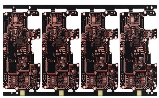
Laser drilling forms microvias in the build-up dielectric. Mechanical drilling may still be used for through holes and larger buried vias, depending on the stackup. After drilling, the holes need debris removal and surface preparation before copper deposition and plating. Via geometry, capture-pad registration, and plating quality all affect interconnect reliability. IPC’s microvia reliability research discusses why stacked microvia structures deserve careful design and qualification.
5. Fill vias when the assembly requires it
For via-in-pad or stacked structures, a specified fill and copper cap may be necessary to create a suitable mounting surface or support a subsequent build-up layer. Do not assume every microvia is filled. State the required via treatment on the fabrication drawing and confirm it with the board and assembly teams, especially under fine-pitch BGAs.
6. Image outer layers and apply the specified finish
After the final build-up cycle, the outer circuitry is imaged and plated or etched according to the selected fabrication flow. Solder mask, legend, and surface finish follow. Choose the finish to suit assembly, shelf-life, and environmental requirements rather than assuming one option fits every design. Fine-pitch pad coplanarity and solder-mask definition should be reviewed with the assembler.
7. Inspect and electrically test the completed boards
Final checks typically include visual or AOI inspection, dimensional and registration checks, and electrical continuity/isolation testing. Additional cross-section, impedance, or thermal reliability evidence should be specified when the design or end use requires it. Ask how coupon results and inspection records will be reported. A good HDI PCB manufacturing process ends with documented acceptance criteria, not merely a delivered board.
What to send for an HDI PCB RFQ
- Fabrication files, drill data, netlist, drawing, and revision identifier.
- Proposed stackup, materials, finished thickness, and impedance targets.
- Microvia layer pairs, stacked or staggered arrangement, and via-fill requirements.
- Minimum trace/space, smallest hole and pad, finish, quantity, and delivery target.
- Any test, inspection, certification, or application-specific reliability requirements.
For more context on material selection and layer structures, see Rogers on PCB stackups. If the stackup is still open, send the design constraints and ask for a manufacturability review before freezing it. Contact KKPCB for an HDI PCB RFQ with your files and target specifications. We can review the requirements and respond with a build approach for your project.
Frequently asked questions
Are all HDI PCBs made with stacked microvias?
No. Staggered microvias and other routing structures can satisfy many designs. The choice depends on component escape, layer count, space, and reliability requirements.
Which step most affects HDI yield?
There is no universal single step. Stackup and via architecture, layer registration, drilling, plating, and inspection interact. A design-for-manufacture review helps expose the main risks for a specific board.
For more technical background on blind, buried, and microvias, see Altium’s via documentation.
