



RO3010 to RT/duroid 5880: 7 Filter Redesign Checks
RO3010 to RT/duroid 5880 is a major material change for a microstrip filter. Rogers lists RO3010 with a process dielectric constant of 10.2 ± 0.30 at 10 GHz and RT/duroid 5880 with a process value of 2.20 ± 0.02. Those values come from defined test methods; the design values used in a specific electromagnetic model may differ. Keeping the old trace widths and gaps while switching laminates is therefore unlikely to preserve the intended filter response.
This guide explains a practical redesign sequence for engineers evaluating that substitution. It focuses on coupled-line filters, but the same discipline applies to other RF structures. Check the current RO3010 product information and RT/duroid 5880 product information before specifying a material. For fabrication options, see our high-frequency PCB service.
1. Freeze the original electrical requirements
Record center frequency, bandwidth, passband ripple, insertion loss, return loss, stopband rejection, power, and temperature range. Preserve the original simulation files and measured results if available. These targets, rather than the old artwork dimensions, are the basis for comparison. Define which values are mandatory and which can change after the material substitution.
2. Compare the full material stackups
For the RO3010 to RT/duroid 5880 change, compare laminate thickness, copper thickness and profile, bonding material, solder mask, and the ground-plane structure. Dk and Df alone do not describe the finished transmission line. Use the material supplier’s appropriate design Dk for the frequency and geometry, then confirm the modeled stackup with the fabricator. Rogers’ laminate properties tool distinguishes process and design data and notes that raw-material test values may not directly represent every microstrip design.
3. Recalculate single-line and coupled-line dimensions
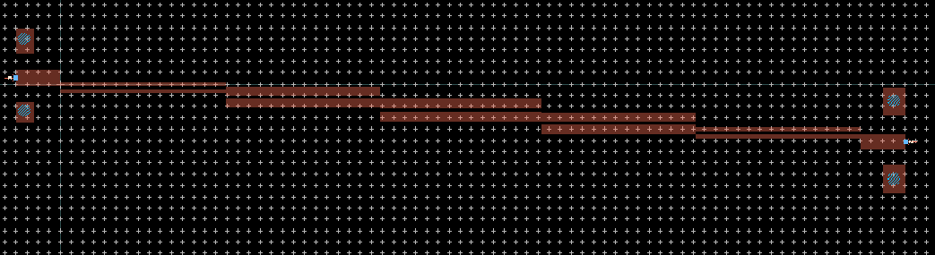
A lower Dk usually changes the physical length and width needed for the same electrical length and impedance. In a coupled-line filter, both even- and odd-mode impedances and the coupling gap matter. Start with an analytical synthesis, then use a field solver or full-wave electromagnetic model that includes the actual copper and dielectric geometry. Do not scale every dimension by one factor; bends, launches, gaps, and end effects may need separate optimization.

4. Check the proposed gaps against fabrication capability
Simulation may produce a very small coupling gap. Ask the PCB manufacturer for achievable trace and space limits at the chosen copper weight and board size, including tolerance and registration. A nominal gap that the shop cannot hold consistently is not a production-ready solution. If the required coupling is too strong for a practical gap, reconsider line geometry, layer structure, or filter topology before release.
5. Model discontinuities and losses
Include connector launches, transitions, bends, pad parasitics, copper roughness, conductor loss, dielectric loss, and the planned finish. Compare insertion loss and return loss across the full operating band, not just at center frequency. Revisit the design under expected material and fabrication tolerances. Our microwave PCB design guide covers related layout considerations.
6. Build and measure a prototype
Make test coupons or a small prototype with the agreed stackup. Measure S-parameters with calibrated fixtures and record the reference planes, environment, and assembly details. Compare measured results with the model; adjust the model or physical design if the shift is repeatable. A simulation that looks similar to the old response does not prove the replacement board will meet specification in production.
7. Release a controlled fabrication package
Once the prototype meets the electrical target, freeze material grade, thickness, copper specification, stackup, geometry, impedance requirements, and test method. Include revision-controlled fabrication files and any allowed substitution rules. The RO3010 to RT/duroid 5880 decision should be documented as a redesign with evidence, rather than an unqualified part swap.
RFQ checklist for a material change
- Original material and stackup, plus the proposed replacement.
- Gerber or ODB++ data, drill files, drawing, netlist, and revision.
- Frequency response targets and S-parameter measurement requirements.
- Minimum trace and gap, copper weight, finish, quantity, and schedule.
- Prototype, coupon, and production acceptance criteria.
Send these details through our RFQ contact page. KKPCB can review the proposed stackup and manufacturability before the filter design is released.
Frequently asked questions
Can RO3010 artwork be used unchanged on RT/duroid 5880?
It should not be assumed. For RO3010 to RT/duroid 5880, dielectric properties differ substantially, so line impedances, coupling, and electrical lengths need new analysis and measurement.
Does lower Df guarantee a better filter?
No. Total response also depends on conductor loss, geometry, transitions, tolerance, and assembly. Evaluate the finished filter against its electrical specification.
