





High-Frequency PCB Routing: 10 Essential Layout Rules
High-frequency PCB routing must control the electromagnetic path of both the signal and its return current. Trace length alone is not enough: reference planes, impedance, via transitions, coupling, materials, power integrity, and fabrication tolerances all affect performance. These ten practical rules help engineers reduce reflections, crosstalk, EMI, and avoidable DFM changes before manufacturing.
What makes PCB routing high frequency?
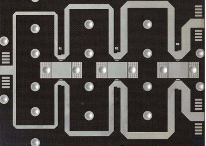
A net can behave as a transmission line even when its clock frequency seems low. The deciding factor is often signal rise and fall time compared with interconnect delay, not an arbitrary 1 GHz boundary. Fast digital edges contain high-frequency energy, while RF and microwave traces intentionally carry high-frequency signals. In both cases, the layout must preserve a defined impedance and continuous return path.
| Routing risk | Typical cause | Design response |
|---|---|---|
| Reflections | Impedance discontinuity or poor termination | Control geometry, stackup, vias, connectors, and termination |
| Crosstalk | Long parallel coupling and field spread | Increase spacing, shorten parallelism, and use close references |
| EMI | Large return loops or common-mode conversion | Maintain reference continuity and pair balance |
| Insertion loss | Dielectric loss, copper roughness, and long routes | Select materials and limit the channel loss budget |
| Power noise | High PDN impedance and poor decoupling placement | Optimize plane pairs, capacitors, and via inductance |
1. Design from edge rate and channel requirements
Start with driver rise time, receiver limits, data rate, frequency content, channel length, connector models, and allowed loss or jitter. A route becomes electrically long when propagation delay is significant relative to the signal transition. Use transmission-line analysis when the interconnect is electrically long, when impedance tolerance is specified, or when simulation shows sensitivity.
2. Keep a continuous return path
Return current follows the path of least impedance, which at high frequency is normally close to the signal trace on its reference plane. Routing over a plane split, void, slot, or poorly connected reference forces a detour and enlarges the loop area. This can increase EMI, crosstalk, and mode conversion.
During high-frequency PCB routing, keep critical traces over an unbroken ground plane whenever possible. If a trace changes layers, place a ground stitching via close to the signal via so return current can transfer between reference planes. When the reference changes between power and ground, use an appropriate nearby return path based on the PDN design rather than assuming the planes are identical at every frequency.
3. Control single-ended and differential impedance
Impedance depends on trace width, copper thickness, dielectric thickness, dielectric constant, solder mask, copper roughness, and the distance to reference planes. Use the fabricator’s finished stackup values, not only nominal laminate data. Prepreg thickness changes with resin content, glass style, copper distribution, and lamination.
Define the impedance target and tolerance for every controlled structure. Identify the reference layer, surface or internal routing, and whether solder mask is included. Request representative impedance coupons and TDR testing when required. Do not compensate trace width in the layout until the fabricator confirms the production stackup.
4. Minimize and model via transitions
Vias add inductance, capacitance, anti-pad discontinuity, and unused stub length. The effect depends on geometry and frequency; a universal value such as “0.5 pF per via” is not reliable for every board. Keep critical transitions short, use nearby ground stitching vias, and maintain consistent anti-pad geometry.
For long through-hole stubs, evaluate backdrilling or blind/buried vias when simulation justifies the cost. Model launches that include pads, vias, anti-pads, reference changes, connectors, and component breakouts. The goal of high-frequency PCB routing is not zero vias, but controlled discontinuities with a valid return path.
5. Control crosstalk with spacing and reference coupling
Crosstalk increases with parallel length and field overlap. Increase spacing between unrelated critical nets, shorten parallel routing, and keep each signal layer close to its reference plane. On adjacent signal layers, use orthogonal preferred directions where practical, but do not treat perpendicular routing as a substitute for a solid reference plane.
Guard traces can help in selected RF layouts only when they are connected to ground with an effective via pitch and do not create new resonances. Random copper beside a trace is not automatically a shield. Use field solving or simulation for tightly coupled structures, sensitive analog nodes, and channels with aggressive spacing.
6. Route differential pairs as a balanced structure
Differential performance depends on individual impedance, differential impedance, pair spacing, reference continuity, skew, and symmetry through vias and connectors. Keep both traces in the same environment, match transitions, avoid unequal stubs, and correct intra-pair skew near the source of the mismatch rather than adding excessive serpentine routing in a noisy area.
Pair members do not need to be as close as manufacturing allows. The correct spacing comes from the impedance target, coupling strategy, routing density, and common-mode requirements. Preserve symmetry around obstacles and use matched ground-via patterns at layer transitions.
7. Use smooth, consistent routing geometry
Modern PCB fabrication does not require 45-degree corners solely for copper adhesion. The electrical concern is the local impedance change and current distribution created by geometry. Use arcs, 45-degree bends, or mitered structures when they help maintain consistent width and spacing. For ordinary digital routing, a well-formed 90-degree corner is often less important than reference continuity, via design, and total channel loss.
Avoid abrupt neck-downs, unnecessary test pads, large pad-to-trace steps, sharp differential asymmetry, and uncontrolled copper pours. Keep RF structures consistent and use electromagnetic simulation for bends, tees, filters, antennas, and launch transitions where small geometry changes affect performance.
8. Design the power distribution network
Place high-frequency decoupling capacitors close to power pins, with short connections and low-inductance power and ground vias. Capacitor value alone does not define performance; package inductance, via inductance, mounting geometry, plane spacing, and the regulator-to-load path determine the impedance profile.
Use a target-impedance approach when rail noise is critical. Closely spaced power and ground planes can add distributed capacitance, but they do not replace discrete decoupling. Check anti-resonances and the full frequency range with simulation or measurement for sensitive processors, converters, RF devices, and high-speed interfaces.
9. Do not split analog and digital ground blindly
Separating analog and digital ground with gaps, beads, or isolated islands can make return paths worse when signals cross the boundary. Many mixed-signal boards perform best with a continuous ground plane, careful component placement, controlled current paths, and separation by functional area. Follow the converter or component manufacturer’s reference design and analyze where return currents flow.
If isolation is required for safety, common-mode control, or architecture, keep signals within their intended domain and cross isolation barriers only through approved components. The high-frequency PCB routing plan should define return paths before traces are placed, not repair them after the layout is complete.
10. Close the loop with materials and fabrication data
Material Dk, dissipation factor, copper roughness, glass weave, moisture, and thickness tolerance affect real channels. Select a suitable system through the KKPCB PCB materials overview and confirm availability with the fabricator. For RF and microwave products, review the KKPCB high-frequency PCB capability page.
- Provide the full stackup with finished copper and dielectric thicknesses.
- List impedance targets, tolerances, reference planes, and coupon requirements.
- Identify critical frequencies, data rates, rise times, loss budgets, and skew limits.
- Define via structures, backdrill depth, surface finish, and material performance.
- Request DFM, stackup, impedance, test, and panelization review before production.
For a broader pre-release audit, use the high-frequency PCB design checks. Consult the applicable edition of IPC-2221, Generic Standard on Printed Board Design, together with interface, product, and customer specifications.
Request a high-frequency PCB routing and DFM review
KKPCB can review high-frequency PCB routing, stackup, controlled impedance, return paths, via transitions, materials, coupons, and fabrication tolerances before production. Send your Gerber or ODB++ package, drill files, stackup, impedance table, interface requirements, material preference, and expected volume through the KKPCB RFQ contact page. A review of high-frequency PCB routing before release reduces redesign risk and improves the quality of the first fabrication build.
