





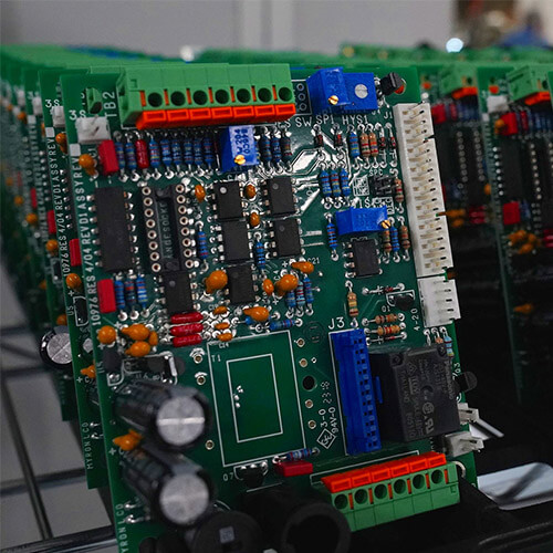
Design concept using multi-layer circuit structure to optimize RF performance
Multi-layer circuit design can improve RF performance when the stackup, return paths, materials, and fabrication limits are planned together. For a filter, antenna feed, or microwave interconnect, the practical question is not simply how many layers fit in the board. It is whether the finished PCB will meet the required insertion loss, isolation, impedance, and repeatability at the operating frequency.
1. Define the RF target before selecting a multi-layer circuit stackup
Record the operating and stopband frequencies, insertion and return loss limits, target impedance, isolation, power, temperature range, and board size. Identify which traces are microstrip, stripline, or grounded coplanar waveguide. These structures have different field distributions and manufacturing sensitivities. A multilayer PCB stackup should be agreed with the fabricator before trace widths and via transitions are finalized.
2. Keep the signal return path controlled
Place a continuous reference plane close to each critical RF trace unless an intentional discontinuity is part of the circuit. A signal changing layers needs a nearby return-path transition, often provided by ground vias. Check connector launches, pads, slots, and layer transitions in the electromagnetic model. The required via spacing and clearance depend on frequency and geometry; they should be verified for the specific design rather than copied from a universal rule.
3. Use a defected ground structure only for a defined function
A defected ground structure (DGS) is a deliberate opening or pattern in a reference plane. It changes the local inductance and capacitance and can help shape a filter response or coupling. It also interrupts the return path and may increase radiation or reduce isolation if used without analysis. In a suitable three-copper-layer structure, a lower ground plane and ground-via connections can help contain fields from a DGS on the middle plane. This benefit depends on the actual layer spacing, materials, geometry, and frequency; it is not guaranteed by adding a layer alone. See the Rogers technical discussion of multilayer DGS circuits for a worked low-pass-filter example.
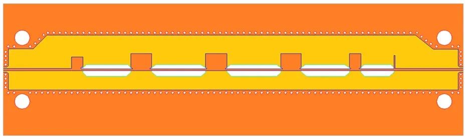
4. Choose laminates and copper with the frequency in mind
Compare design dielectric constant (Dk), loss factor (Df), thickness tolerance, copper roughness, thermal behavior, and availability at the intended frequency. A material change can alter characteristic impedance and even- and odd-mode phase velocities in coupled lines. For mixed-material boards, confirm the bonding system and lamination process as well as the electrical model. KKPCB’s PCB materials information is a starting point; the final choice should follow the RF specification and a manufacturable stackup.
5. Check DGS and coupled-line features against fabrication limits
Small etched gaps, narrow traces, plated vias, and layer registration all have tolerances. A simulated multi-layer circuit may perform differently after etching or lamination changes its critical dimensions. Ask the fabricator to review minimum trace and gap widths, copper weight, dielectric thickness, via aspect ratio, and registration before releasing the artwork. Specify the parameters that affect RF behavior rather than relying on nominal layer count alone.
6. Simulate and measure the complete RF path
Model the intended stackup, launches, vias, adjacent structures, and DGS where relevant. Include material and dimensional tolerances in a sensitivity check. For the prototype, measure S-parameters with a suitable calibration and fixture strategy, then compare the results with the simulated passband, stopband, and isolation. Investigate differences before volume production. The same workflow applies to filters and to antenna feeds, although their acceptance metrics differ. For another practical design perspective, read our high-frequency PCB design guide.
7. Prepare a useful RFQ package
To assess a multi-layer circuit for RF fabrication, provide Gerber or ODB++ files, the proposed stackup, laminate preference, operating frequency, controlled-impedance targets, critical tolerances, surface finish, quantity, and test requirements. If a DGS or mixed-material construction is essential, identify it explicitly. KKPCB can review the manufacturability of the supplied design and discuss a prototype plan. Contact KKPCB for an RF PCB quotation with these files and requirements.
Frequently asked questions
Does adding more layers automatically reduce RF loss?
No. Loss depends on the transmission-line structure, dielectric and conductor losses, dimensions, transitions, and frequency. Additional layers can improve routing and shielding options, but the full stackup still needs validation.
Can a defected ground structure be used in every RF PCB?
No. A DGS should serve a defined electrical purpose. Model its effect on return current, radiation, isolation, and manufacturability, then verify the prototype.
