



Innovative printing solutions for front-end RF module packaging
RF module packaging combines small passives, filters, switches, amplifiers, and interconnects in a limited footprint. Printing solder paste for a dense RF front-end or system-in-package (SiP) assembly is difficult because tiny stencil apertures must deliver repeatable deposits while nearby pads must avoid bridging. The RF substrate also needs suitable loss and Dk control; see Rogers guidance on PCB materials for 5G. A useful process plan starts with the package design and verification criteria, then selects stencil, paste, inspection, and reflow settings as one system.
1. Define the assembly and RF requirements
List the smallest passive package, flip-chip or copper-pillar geometry, pad finish, aperture spacing, component height, reflow limits, cleaning requirements, and acceptable voiding. Also identify the RF path and any sensitive ground or matching structures. The assembly process must protect both solder-joint integrity and the electrical function of the finished module. A PCB layout and design-for-manufacture review can flag clearance and pad-design problems before a stencil is ordered.
2. Understand conventional and single-pass printing
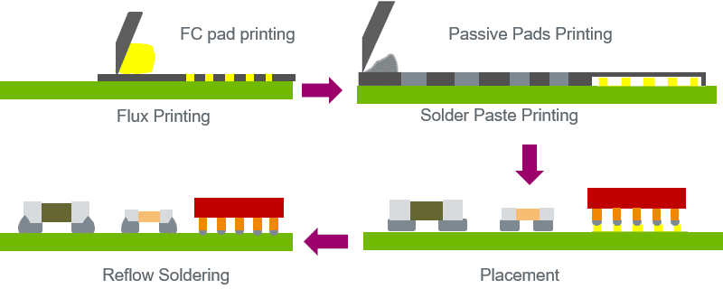
A conventional flow may apply flux to flip-chip sites and solder paste to passive-component pads in separate steps. A single-pass approach attempts to print a compatible solder paste for both groups in one operation. It can simplify the flow, but it is not suitable by default for every product. Paste chemistry, stencil design, flip-chip process, and reflow profile must all be qualified. Heraeus describes an all-in-one printing approach for advanced packaging; its product data should be treated as supplier-reported performance, not as a universal yield guarantee.
3. Match stencil apertures to paste release
Fine openings can retain solder paste instead of transferring a consistent deposit. Evaluate aperture width, area ratio, stencil thickness, wall quality, and spacing together. Type 7 powder is one option for very fine features, but the powder designation alone does not establish a stable process window. In a published Heraeus AP520 T7 fact sheet, the supplier reports tests at a 55 µm aperture under specified stencil and pad conditions. Those results should be requalified for a different board, finish, stencil, and reflow line.
4. Use SPI data to control deposits
Solder paste inspection (SPI) can measure deposit volume, area, height, and position. Set limits for the actual pad types, then review trends across the stencil rather than judging one print in isolation. Track missing deposits, bridging, and variation at the smallest apertures. If a process uses a separate flux-printing step, confirm that the inspection method can detect that material reliably. For production, retain the measurements that demonstrate the selected window is stable.
5. Check warpage, wetting, and reflow
Non-wet opens can result from poor contact between a bump and pad, insufficient wetting, or movement during reflow. Substrate warpage and coplanarity must be evaluated with the paste and thermal profile. More paste is not automatically a cure: excess volume can create bridging or voids. Use cross-sections, X-ray where appropriate, and electrical tests to confirm joint quality. Document the cleaning or residue requirements for the chosen flux system.
6. Separate supplier test results from your own qualification
For RF module packaging, published material data are helpful starting points, but RF module packaging performance depends on the complete process. Before release, run a representative test vehicle with the intended substrate, pad finish, components, stencil, paste, equipment, and reflow profile. Define pass criteria for print consistency, solder defects, RF performance, and reliability. IPC research on fine-feature solder paste inspection provides further context on why mixed pad sizes challenge conventional printing rules.
7. Prepare an actionable manufacturing inquiry
For an RF module packaging inquiry, send assembly drawings, Gerber or ODB++ files, a BOM, component and bump drawings, pad finish, stencil constraints, reflow limits, volume forecast, inspection criteria, and RF test requirements. KKPCB offers PCB assembly and SMT assembly services. For a dense RF module project, ask the team to review which fabrication and assembly steps fit the supplied design. Contact KKPCB for an RFQ with the technical package; any specialized SiP or flip-chip step should be confirmed during that review.
Frequently asked questions
Does Type 7 paste guarantee fine-pitch printing?
No. Aperture design, stencil quality, pad finish, environment, and printer setup also affect release and defects.
Can one-pass printing replace every two-step RF module process?
No. Confirm compatibility with the flip-chip attach method, passive components, inspection, cleaning, and reflow requirements on a representative test vehicle.
