


High-Frequency PCB Reliability: 7 Factors to Validate
High-frequency PCB reliability depends on more than a laminate’s room-temperature dielectric constant. A board must maintain acceptable electrical and mechanical performance through fabrication, assembly, storage, and its operating life. Heat, moisture, oxidation, copper geometry, and via integrity can each change the result. The practical question for an RF engineer is which conditions to specify and which evidence to request from the PCB manufacturer.
This guide explains the main risks and gives a qualification checklist. It applies to RF and microwave boards using PTFE-based or hydrocarbon ceramic laminates, but the right limits depend on the exact material, circuit structure, and product environment. Review our high-frequency PCB service for fabrication options and our PCB surface finish guide for assembly-related choices.
1. Define the actual operating conditions
Record the frequency band, maximum continuous board temperature, thermal cycles, humidity, expected service life, and any high-power hot spots. These values are more useful than a generic requirement for a “reliable RF board.” Identify which measurements matter most: insertion loss, phase, impedance, resonant frequency, or isolation. Set acceptance limits and test conditions before comparing materials. High-frequency PCB reliability cannot be inferred from one Dk or Df number.
2. Check dielectric stability at temperature and humidity
Dielectric constant (Dk) and dissipation factor (Df) influence impedance and loss. The values in a datasheet have defined measurement methods and conditions; they are not guaranteed circuit values at every frequency or temperature. Ask the laminate supplier for data near the intended operating conditions, then validate the finished structure. Moisture uptake and drying can also shift RF measurements, particularly when comparing test coupons taken under different conditions. Rogers’ laminate properties tool provides material data and notes limitations for design use.
3. Evaluate long-term heat and oxidation exposure
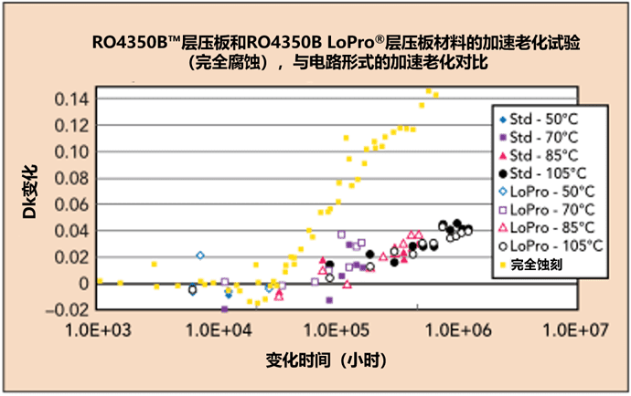
Some hydrocarbon-based materials can change dielectric properties after prolonged exposure to an oxidative environment, especially at elevated temperature. The effect depends on formulation and circuit design, and it should not be assumed to occur at the same rate in every product. Rogers’ RO4000 fabrication guidelines recommend evaluating each material and design over the intended product life. Where aging is a concern, request supplier evidence and run a test that reflects your own board geometry and environment.
4. Control copper and transmission-line geometry
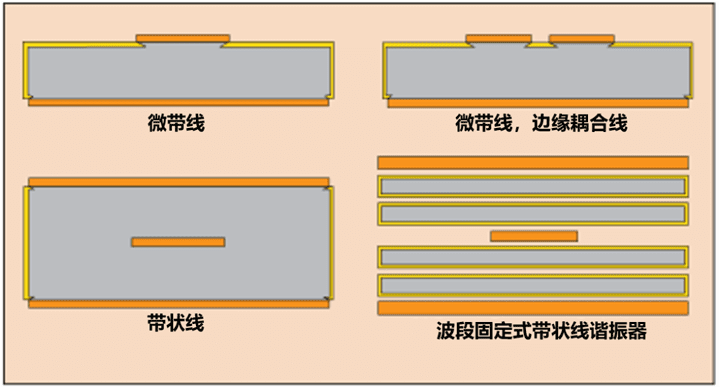
Conductor width, gap, thickness, copper profile, and registration affect impedance and loss. At microwave and millimeter-wave frequencies, small fabrication variation can have a larger electrical effect. Specify the target impedance and tolerance with the stackup, reference layers, finish, and any controlled-impedance coupons. A microstrip, stripline, and grounded coplanar waveguide do not expose fields to the same material regions, so choose representative test structures. See our microwave PCB design guide for layout considerations.
5. Review thermal expansion and plated-hole integrity
Temperature cycling creates mechanical stress where the laminate, copper, and plated holes expand differently. Risk grows when stackup, board thickness, hole aspect ratio, or assembly profile is pushed beyond the selected process window. Give the fabricator the required layer count, finished thickness, hole sizes, and thermal exposure. Discuss suitable coupons, cross sections, and cycling tests for the application. The acceptance plan should reflect the finished PCB rather than relying only on raw laminate data.
6. Consider assembly and surface protection
Reflow can impose short but intense thermal exposure. Confirm that the selected materials and finished board structure can tolerate the specified assembly profile; do not assume a favorable laminate datasheet alone qualifies the full board. For high-frequency PCB reliability, surface finish, solder mask, cleanliness, and storage conditions also affect assembly yield and long-term performance. State any special finish, handling, or cleanliness requirement on the drawing.
7. Verify the board with representative evidence
A useful plan may include electrical continuity and isolation, impedance coupons, RF insertion-loss or resonator measurements, microsections, and environmental cycling. For high-frequency PCB reliability, choose tests according to failure risk and customer specification. Compare baseline and post-stress results using the same fixture and conditioning procedure. Record lot, material revision, stackup, and test conditions so a future change can be investigated. This is how high-frequency PCB reliability becomes a measurable requirement.
What to include in an RF PCB quote request
- Gerber or ODB++ files, drill data, netlist, drawing, and revision.
- Frequency range, impedance targets, insertion-loss or phase limits, and test method.
- Laminate preference or performance targets for Dk, Df, thickness, and copper profile.
- Operating temperature, humidity, service-life target, power level, and assembly profile.
- Required inspection, environmental qualification, documentation, quantity, and delivery target.
Send KKPCB your RF PCB files for a manufacturability and quote review. We can discuss the stackup and the evidence needed for your specific reliability target.
Frequently asked questions
Is the lowest-Df laminate always the most reliable?
No. Electrical loss is one selection factor. Mechanical fit, processing, environmental exposure, availability, and the finished board test plan also matter.
Can accelerated aging predict exact field life?
It can help compare risks under a defined model and test setup. Extrapolation has limits; validate assumptions against the actual material, circuit geometry, and operating environment.
