






Rigid PCB Manufacturing: 8 Essential Material and DFM Choices
Rigid PCB manufacturing converts a stable laminate stackup into a mechanically fixed printed circuit board that supports components, controlled interconnects, and repeatable assembly. Reliable results depend on more than choosing FR-4: layer count, laminate performance, copper weight, hole structure, surface finish, thermal requirements, tolerances, and test strategy must match the product. This guide explains eight decisions buyers and design engineers should define before requesting a rigid PCB quotation.
What is a rigid PCB?
A rigid PCB uses a non-flexing laminate structure, most commonly glass-reinforced epoxy, to hold its shape during installation and service. It can be single-sided, double-sided, or multilayer. Rigid describes the mechanical construction, not the electrical complexity: a rigid board may carry simple low-frequency control circuits or high-speed, RF, high-current, and high-density interconnects.
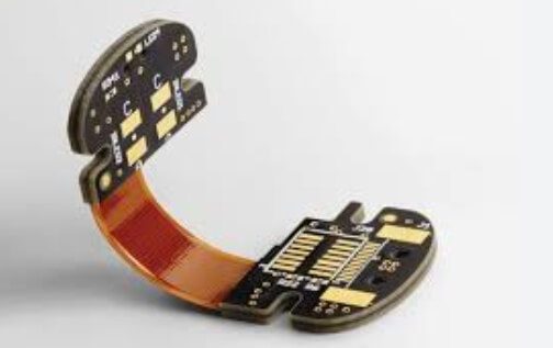
Rigid boards are different from rigid-flex PCBs, which combine rigid and flexible regions in one interconnected structure. Choose rigid construction when the board does not need to bend and when connectors, wiring, or multiple boards can meet the mechanical architecture.
1. Select the board type and layer count
| Rigid PCB type | Typical use | Main design consideration |
|---|---|---|
| Single-sided | Simple controls, indicators, power distribution | Low routing density and one copper side |
| Double-sided | Industrial controls, consumer products, power electronics | Through-hole interconnection and two routing sides |
| Multilayer | Processors, communications, automotive, medical, RF | Stackup, impedance, plane strategy, registration |
| Metal-core rigid PCB | LEDs and selected power applications | Dielectric thermal resistance and electrical isolation |
| HDI rigid PCB | Fine-pitch BGAs and compact high-I/O products | Microvias, sequential lamination, yield, qualification |
Use the lowest layer count that completes routing while preserving continuous reference planes, power distribution, thermal spreading, and manufacturable spacing. Adding layers can improve routing and EMC but also changes cost, thickness, lamination complexity, and lead time. A rigid PCB manufacturing review should confirm that the proposed layer count supports both layout and fabrication.
2. Choose laminate materials from performance requirements
Standard FR-4 is suitable for many products, but “FR-4” is a broad material class rather than one fixed electrical or thermal specification. Define glass-transition temperature, decomposition temperature, z-axis expansion, dielectric constant, dissipation factor, moisture performance, flammability, and CAF resistance as needed. High-Tg material can improve margin for lead-free assembly and thermal cycling, but Tg alone does not guarantee reliability.
High-speed and RF designs may require lower loss, stable Dk, controlled copper roughness, or specialized hydrocarbon/ceramic and PTFE systems. High-voltage products need suitable creepage, clearance, dielectric thickness, and insulation performance. Select candidates through the KKPCB PCB materials overview and agree on an approved-substitute process before routing is frozen.
3. Specify finished copper weight correctly
Base copper and finished copper are not the same. Outer layers normally receive additional plated copper during through-hole processing, while inner-layer copper is defined by the starting foil and etching result. State finished copper requirements per layer and account for trace width, current, temperature rise, etch compensation, and minimum spacing.
Heavy copper supports higher current and heat spreading but makes fine features and uniform etching more difficult. Thin copper supports finer routing but may require wider conductors for current. Use appropriate current-capacity analysis, thermal simulation, and derating instead of choosing copper weight from a generic table alone.
4. Define the stackup and controlled impedance
A multilayer stackup should be electrically and mechanically balanced. Place critical signal layers next to continuous reference planes, keep important power/ground pairs suitably spaced, and use symmetric dielectric structures where possible. The fabricator must confirm available cores, prepregs, glass styles, pressed thicknesses, copper weights, and total thickness tolerance.
Controlled impedance depends on trace geometry, finished copper, dielectric thickness, Dk, solder mask, and copper roughness. Provide the target, tolerance, layer, reference plane, and coupon requirements. The final trace adjustment should use the approved production stackup. Many rigid PCB manufacturing problems begin when the designer routes against nominal material data that differs from the pressed construction.
5. Use manufacturable holes and via structures
Minimum mechanical drill, finished hole, annular ring, aspect ratio, and hole-to-copper clearance depend on board thickness, copper thickness, plating, material, layer count, and reliability class. Extreme claims such as a universal 0.002-inch mechanical drill or 35:1 plated-hole aspect ratio should not be treated as standard capability. Confirm limits for the actual stackup and production volume.
Blind and buried vias, laser microvias, via-in-pad filling, resin-filled through vias, and backdrilling can solve specific density or signal-integrity problems. Each option adds process steps and qualification requirements. Use advanced vias only when the electrical or mechanical benefit justifies cost and risk.
6. Match the surface finish to assembly and service
Common finishes include lead-free HASL, ENIG, ENEPIG, immersion silver, immersion tin, OSP, hard gold on connector fingers, and selected wire-bond finishes. The decision depends on pad flatness, solderability, storage, reflow cycles, contact wear, wire bonding, fine pitch, corrosion environment, and cost.
No finish is best for every design. ENIG provides flat pads and broad assembly compatibility; ENEPIG can support mixed soldering and selected wire bonding; hard gold is used on durable contacts rather than ordinary solder pads. Review the PCB surface treatment guide before specifying the finish.
7. Define thermal and mechanical requirements
Provide operating and storage temperature, assembly profile, thermal cycles, vibration, shock, humidity, chemical exposure, and expected service life. High-Tg FR-4 may help with thermal margin, but copper distribution, z-axis expansion, plated-hole design, component heat, and enclosure airflow still control reliability.
For power products, define copper temperature rise, heat sources, thermal vias, interface materials, and any metal base or heat spreader. For thin or large boards, specify bow and twist requirements and maintain copper balance. Panelization, rails, tooling holes, breakaway method, and assembly support should be reviewed with the manufacturer.
8. Complete DFM, testing, and RFQ data
A professional rigid PCB manufacturing RFQ should include more than Gerber files. The engineering package should explain materials, performance, tolerances, inspection, test, and the end-use environment so the supplier can identify conflicts before production.
- Gerber or ODB++ data, NC drill files, netlist, drawings, and revision.
- Layer stackup, finished copper, material requirements, and total thickness tolerance.
- Minimum features, hole structures, filled/capped vias, backdrill, and depth tolerances.
- Impedance targets, reference layers, coupons, and TDR acceptance limits.
- Surface finish, solder mask, legend, edge plating, gold fingers, and special processes.
- IPC class or customer criteria, electrical test, microsections, traceability, and reports.
- Panelization, assembly method, annual volume, packaging, and required lead time.
For formal qualification and performance requirements, consult the applicable edition of IPC-6012, Qualification and Performance Specification for Rigid Printed Boards, together with IPC-2221, product standards, and customer requirements.
Request a rigid PCB manufacturing and DFM review
KKPCB supports prototype and production rigid PCB manufacturing for single-sided, double-sided, multilayer, high-frequency, HDI, heavy-copper, and metal-core requirements. Send the complete data package through the KKPCB RFQ contact page. Our engineering team can review materials, stackup, impedance, holes, copper, surface finish, panelization, testing, and assembly risk. A complete rigid PCB manufacturing review protects yield, reliability, and total project cost without relying on copied or unrealistic capability figures.
