




HDI PCB Applications: 7 Industries and Build-Up Choices
HDI PCB applications use microvias, fine lines, thin dielectrics, and sequential build-up structures to place more interconnects in less area while controlling signal and power performance. HDI is valuable when component pitch, board size, routing density, or electrical requirements exceed the practical limits of a conventional through-hole multilayer board. This guide explains seven major application areas, how 1+N+1 and 2+N+2 structures differ, and what engineers should include in an HDI manufacturing RFQ.
Why products use HDI PCB technology
High-density interconnect technology is not defined only by a high layer count. It combines microvias, blind and buried vias, fine traces and spaces, thin dielectric layers, capture-pad reduction, and sequential lamination. These features allow escape routing from fine-pitch BGAs, shorten critical interconnects, reduce via parasitics, and support smaller board outlines. The electrical benefit depends on the complete stackup and return-path design; HDI does not automatically make every signal faster or every board more reliable.
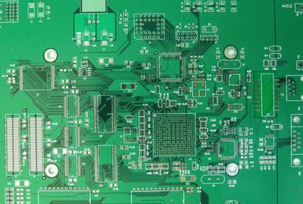
Typical HDI PCB applications need one or more of the following: compact size, high I/O count, controlled impedance, reduced via stubs, low inductance, lightweight construction, or dense component placement. The designer should compare those benefits with extra lamination cycles, tighter registration, microvia reliability limits, inspection, testing, and yield.
Choose the correct HDI build-up structure
| Structure | Meaning | Typical use | Main consideration |
|---|---|---|---|
| 1+N+1 | One build-up layer on each side of an N-layer core | Moderate BGA escape and compact products | One sequential lamination cycle after the core |
| 2+N+2 | Two build-up layers on each side | Higher routing density and smaller BGA pitch | More lamination, registration, and microvia interfaces |
| 3+N+3 or higher | Three or more build-up layers per side | Very dense computing, modules, or advanced systems | Reliability, yield, cost, and supplier capability |
| Any-layer HDI | Laser microvias can connect selected adjacent layers throughout the structure | Maximum routing flexibility and miniaturization | Multiple sequential processes and strict qualification |
The notation describes build-up layers around a conventional core; it is not a universal guarantee of via type or capability. A 2+N+2 board may use staggered microvias, stacked microvias, skip vias, buried vias, or combinations. The final construction must show every via start and stop layer, copper thickness, dielectric thickness, fill and cap requirement, and lamination sequence. Review KKPCB’s HDI PCB manufacturing process for the fabrication sequence.
7 major HDI PCB applications
1. Smartphones, wearables, and compact consumer devices
Mobile and wearable products combine processors, memory, RF front ends, sensors, cameras, power management, and dense connectors in a small enclosure. HDI allows via-in-pad escape, smaller capture pads, short interconnects, and thinner boards. Mechanical bending, battery clearance, antenna keep-outs, thermal paths, and assembly rework must be considered with the electrical layout.
2. High-performance computing and networking
Servers, switches, accelerator cards, and embedded computing platforms use large BGAs and high-speed serial channels. HDI can reduce via-stub length, improve breakout density, and create shorter transitions. Channel performance still depends on low-loss materials, copper roughness, reference continuity, connector models, and validated insertion-loss and return-loss budgets.
3. Automotive electronics
ADAS controllers, cameras, radar modules, infotainment, domain controllers, and compact power electronics are important HDI PCB applications. Material selection and microvia qualification must account for temperature cycling, vibration, humidity, long service life, and automotive quality requirements. Do not assume a consumer-grade HDI construction is automatically suitable for under-hood or safety-related service.
4. Medical electronics
Portable diagnostic equipment, imaging systems, monitoring devices, surgical instruments, and implant-support electronics may require miniaturization and reliable high-I/O interconnects. Risk management, traceability, cleanliness, test coverage, and the applicable medical-device controls are as important as routing density. HDI enables compact layouts but must be qualified for the real sterilization, temperature, and service environment.
5. Aerospace and defense systems
Avionics, radar, communications, navigation, and compact mission electronics use HDI when size, weight, and performance are critical. These designs often require controlled materials, lot traceability, coupon testing, microsections, environmental qualification, and strict change control. The accepted via structure should be based on qualified supplier capability rather than maximum theoretical density.
6. Industrial automation and robotics
Machine vision, motion control, robotics, compact controllers, and industrial sensors benefit from dense processing and I/O. For these HDI PCB applications, review vibration, conductive contamination, thermal cycling, connector loading, service access, and conformal coating. HDI may reduce enclosure size while supporting local processing close to sensors and actuators.
7. RF modules and advanced embedded systems
RF front-end modules, phased-array controls, IoT gateways, and compact embedded platforms may use microvias to shorten transitions and preserve routing area. RF performance depends on via inductance, anti-pad geometry, ground-via placement, dielectric properties, copper roughness, and shielding. Electromagnetic simulation and test coupons are appropriate when the transition is performance-critical.
Microvia design and reliability rules
IPC terminology generally identifies a microvia as a blind structure with a maximum diameter of 0.15 mm and a depth-to-diameter aspect ratio not exceeding 1:1. Supplier limits may be tighter. Laser drilling is the dominant process, but the finished via also depends on desmear, seed metallization, copper plating, filling, planarization, and cap plating.
- Prefer staggered microvias when routing permits because they avoid a stacked interface.
- Use stacked microvias only with a qualified fill and plating process and clear reliability requirements.
- Specify via-in-pad fill, planarization, and cap plating when components mount over the via.
- Keep microvia aspect ratio, capture pad, annular ring, and dielectric thickness within supplier capability.
- Define coupons, microsections, thermal stress, and acceptance criteria for the product class.
The most reliable HDI PCB applications avoid unnecessary stacked levels. Each interface adds manufacturing complexity and can concentrate stress during reflow and thermal cycling. Use the simplest via architecture that completes escape routing and meets channel performance.
Materials, impedance, and signal integrity
Thin HDI dielectrics help form small laser microvias and tightly coupled impedance structures, but pressed thickness varies with resin content, glass style, copper distribution, and lamination. Impedance calculations must use the fabricator’s finished values. For high-speed designs, review dielectric loss, Dk variation, copper roughness, glass weave, skew, insertion loss, and return-path continuity through every layer transition.
Select materials from the KKPCB PCB materials overview and confirm availability before final routing. An approved substitute process should control electrical, thermal, and reliability properties rather than accepting a nominally similar laminate by name alone.
HDI manufacturing RFQ and DFM checklist
Before releasing HDI PCB applications for quotation, provide the complete stackup and via architecture. A fabrication package that only marks holes as “laser vias” leaves critical reliability and cost decisions undefined.
- Show every core, prepreg, build-up dielectric, and finished copper thickness.
- Identify each blind, buried, stacked, staggered, skip, filled, capped, or backdrilled via.
- State minimum trace/space, pad size, hole size, aspect ratio, and registration requirement.
- Provide controlled-impedance structures, references, tolerance, and coupon requirements.
- Define material performance, surface finish, board thickness, bow/twist, and test class.
- Include BGA pitch, via-in-pad locations, assembly profile, expected thermal cycles, and end-use environment.
- Request stackup review, DFM feedback, microsections, electrical test, and reliability testing as applicable.
Use the HDI PCB design checklist before data release. A structured review of HDI PCB applications ensures that density, via architecture, materials, signal integrity, and qualification requirements match the product rather than an outdated market assumption.
For formal design definitions and structure rules, consult the applicable edition of IPC-2226, Sectional Design Standard for High Density Interconnect Printed Boards, together with the product class and customer qualification requirements.
Request an HDI PCB build-up and DFM review
KKPCB supports prototype and production HDI PCB applications with sequential lamination, laser microvias, via-in-pad filling, controlled impedance, and electrical testing. Send your Gerber or ODB++ data, drill files, stackup, impedance table, BGA pitch, via map, material requirements, assembly profile, and expected volume through the KKPCB RFQ contact page. Our engineers can recommend a manufacturable 1+N+1, 2+N+2, or advanced structure before production.
