


What Is a High-Frequency PCB? 7 Essential Design Fundamentals
What is a high-frequency PCB? It is a printed circuit board engineered to carry radio-frequency or other fast-changing signals while controlling impedance, insertion loss, return loss, crosstalk, radiation, and phase behavior. Frequency alone does not create a universal boundary. A board becomes a high-frequency design when ordinary interconnect assumptions no longer protect signal integrity and the traces, vias, reference planes, laminate, copper profile, and connectors must be treated as part of the electrical circuit.
What is a high-frequency PCB in practical terms?
Answering what is a high-frequency PCB in practical terms begins with the interconnect behavior. Engineers often use “RF PCB,” “microwave PCB,” and “high-frequency PCB” interchangeably, but their emphasis differs. RF and microwave boards normally handle intentionally generated radio signals, while a digital board can also demand high-frequency methods when its edge rate is fast enough. The critical question is not only the clock frequency. A fast rise time contains high-frequency energy, so even a modest data rate can create reflections and electromagnetic interference when the interconnect is electrically long.
A useful design test is to compare signal rise time with propagation delay. If the trace delay is a meaningful fraction of the edge time, model the route as a transmission line. This is why high-frequency PCB design covers both RF front ends and high-speed digital interfaces.
Seven essential high-frequency PCB fundamentals
1. Controlled impedance begins with the production stackup
Trace impedance depends on finished copper thickness, trace width, dielectric thickness, dielectric constant, solder mask, copper roughness, and the geometry of nearby reference planes. A generic calculator using nominal material data is only a starting point. The PCB manufacturer must confirm available cores, prepregs, glass styles, pressed thicknesses, etch compensation, and impedance coupon requirements before the layout is released.
2. Material loss and Dk stability matter
Material choice is central to what is a high-frequency PCB and how it performs. Standard FR-4 may be acceptable for short routes or lower-loss budgets, but demanding RF and microwave circuits often need laminates with lower dissipation factor, stable dielectric constant, controlled copper roughness, and predictable performance over frequency and temperature. Material selection should be based on insertion-loss budget, operating frequency, phase stability, thermal environment, fabrication method, availability, and cost—not on the label “high Tg” alone.
Compare candidate systems in the KKPCB PCB materials guide. For hybrid stackups, confirm resin compatibility, lamination temperature, z-axis expansion, drill behavior, and bond strength with the fabricator.
3. Every signal needs a continuous return path
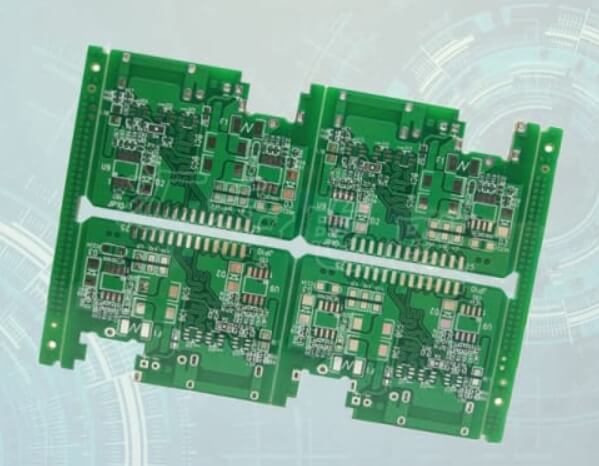
High-frequency current follows the path of lowest impedance, normally close to the signal trace on its reference plane. Gaps, slots, plane changes, and poorly placed stitching vias increase loop area and can cause radiation, crosstalk, and common-mode conversion. Avoid routing critical signals across plane splits. When a route changes layers, place an appropriate ground return via near the signal via so the return current can transition without a long detour.
4. Routing geometry controls coupling and discontinuities
Keep critical routes short, maintain the designed width and reference, and separate aggressors according to stackup and crosstalk analysis. Smooth bends can be useful at microwave frequencies, but a 90-degree corner is not automatically the dominant problem in every design. Pad transitions, connector launches, stubs, via barrels, reference changes, and unexpected trace-width variations often create larger discontinuities. The high-frequency PCB routing guide explains practical return-path, via, and spacing rules.
5. Vias and launches must be designed as structures
A via adds inductance, capacitance, an unused barrel stub, and a reference-plane transition. At higher frequencies these effects can create resonances and excess loss. Optimize drill and pad geometry, use nearby ground vias, minimize layer transitions, and consider backdrilling or blind vias when the simulated or measured benefit justifies the added process. Connector launches should be co-designed with the board stackup and verified through field-solver or electromagnetic simulation for demanding channels.
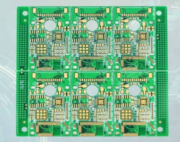
6. Fabrication tolerances affect electrical performance
Etching changes trace width and sidewall shape. Lamination changes dielectric thickness. Copper plating, solder mask, registration, resin flow, and surface finish also influence the final structure. Therefore, impedance and loss targets should include realistic manufacturing tolerances. Share the target impedance, allowed tolerance, reference layer, test frequency or method, coupon design, and acceptance criteria. A professional high-frequency PCB manufacturer should review the production stackup rather than manufacture from an unverified nominal drawing.
7. Verification must match the risk
Verification completes the practical answer to what is a high-frequency PCB. Use simulation before fabrication and measurements after fabrication. Depending on the product, verification may include impedance coupons and TDR, insertion-loss testing, vector network analyzer measurements, time-domain reflectometry, microsection analysis, automated optical inspection, electrical test, and functional RF testing. Define the required reports and pass/fail limits in the RFQ instead of assuming that every board receives the same level of testing. For general printed-board design principles, consult the current IPC-2221 generic design standard and the applicable product-specific requirements.
High-frequency PCB material comparison
| Material family | Typical reason to use it | Key review items |
|---|---|---|
| Standard or high-performance FR-4 | Cost-sensitive digital and selected RF designs | Loss budget, Dk variation, glass weave, copper roughness |
| Low-loss hydrocarbon/ceramic | RF, microwave, antennas, high-speed channels | Dk/Df by test method, thermal expansion, processing compatibility |
| PTFE-based laminate | Low loss and stable microwave performance | Dimensional stability, drilling, surface treatment, bondply system |
| Hybrid multilayer | RF performance only where needed | Lamination compatibility, CTE, resin flow, registration, reliability |
No single laminate is best for every high-frequency PCB. Use supplier data measured with a relevant test method, then validate the selected construction with the fabricator. Published Dk values from different methods are not always directly interchangeable.
Where are high-frequency PCBs used?
- 5G infrastructure, Wi-Fi, Bluetooth, satellite, and point-to-point radios.
- Radar, phased-array antennas, aerospace, defense, and navigation systems.
- Automotive radar, ADAS sensors, vehicle communications, and charging systems.
- Medical imaging, instrumentation, scientific equipment, and test systems.
- High-speed computing, networking, data converters, and SerDes interfaces.
- Industrial sensing, telemetry, IoT gateways, and precision measurement.
High-frequency PCB RFQ checklist
- Gerber or ODB++ data, NC drill files, netlist, fabrication drawing, and revision.
- Approved laminate and acceptable substitutions with Dk, Df, Tg, thickness, and copper requirements.
- Final stackup, finished copper, total thickness, controlled-impedance targets, and tolerance.
- Minimum trace/space, drill sizes, via structures, backdrill details, and aspect-ratio requirements.
- Surface finish, solder mask, special plating, edge treatment, and panelization.
- Operating frequency, power, environment, reliability class, and assembly profile.
- TDR, loss, RF, microsection, electrical-test, inspection, and documentation requirements.
Frequently asked questions
At what frequency does a PCB become high frequency?
There is no universal cutoff. The need for transmission-line methods depends on edge rate, route length, loss budget, geometry, and system requirements. RF designs above hundreds of megahertz commonly need careful control, but fast digital edges can require the same methods at lower clock rates.
Is high-Tg FR-4 automatically a high-frequency material?
No. Tg describes a thermal transition, not RF loss. A high-Tg material can still have a dissipation factor or Dk stability unsuitable for a demanding channel. Evaluate electrical, thermal, mechanical, processing, and supply requirements together.
Does every high-frequency PCB require PTFE?
No. Many products can use an appropriate FR-4 or hydrocarbon/ceramic system. PTFE is selected when its low-loss or stability benefits are required and the fabrication process, mechanical design, cost, and supply chain support it.
Request a high-frequency PCB engineering review
KKPCB supports RF, microwave, high-speed digital, multilayer, hybrid-laminate, impedance-controlled, and advanced-via projects. Send your stackup, material requirements, impedance table, fabrication files, test limits, volume, and application details through the KKPCB RFQ contact page. Our engineering team can review material availability, stackup feasibility, return paths, via transitions, impedance coupons, tolerances, and test strategy before production.
In short, the answer to what is a high-frequency PCB is not merely “a board operating above a certain frequency.” It is a controlled interconnect system whose materials, geometry, reference paths, transitions, fabrication tolerances, and verification plan are engineered together.
